The Mystery of the Failing Wafer
Imagine a semiconductor fabrication facility where everything seems perfect. The cleanroom is rated to the highest standards, the technicians are in full bunny suits, and the ultrapure water (UPW) system is showing optimal readings. Yet, when the latest batch of wafers comes off the line, the yield is disastrous.
Somewhere in the complex web of pipes, valves, and fittings, an invisible "phantom" is at work. Microscopic particles—some no larger than a few nanometers—are hitching a ride on the process chemicals, landing on the silicon, and short-circuiting millions of dollars in potential revenue.
For many engineers, this is a recurring nightmare. You’ve checked the chemicals and the environment, so why is the contamination still there?
The Frustrating Search for "Good Enough"
When contamination strikes, the initial response is often to look at the "big" factors. You might swap out your chemical suppliers or double-filter your etching solutions. But when the yield doesn't improve, the focus shifts to the fluid handling system.
Many labs and fab plants attempt to solve this by using standard plastic valves and tubing, assuming that "chemical resistance" is the only metric that matters. They choose generic polymers that don't melt when exposed to hydrofluoric acid (HF) or aggressive photoresist strippers.
However, this "good enough" approach often leads to a cycle of frustration. You might see:
- Unexplained Particle Spikes: Even though the fluid going in is clean, the fluid coming out of the valve is not.
- Ionic Leaching: Trace metals from the valve body "migrate" into the ultrapure water, altering the electrical properties of the wafer.
- Clogged Lines: Residues from Chemical Mechanical Planarization (CMP) slurries begin to build up in "dead zones" within the valves, eventually breaking loose and ruining a batch.
These issues don't just cause technical headaches; they lead to project delays, astronomical costs in scrapped materials, and a loss of competitive edge in an industry where "purity" is the primary currency.
The Root Cause: Why "Chemically Inert" Isn't "Ultra-Pure"
To solve the mystery, we have to look deeper than just whether a material survives a chemical bath. The secret lies in the difference between chemical resistance and contamination control.
In semiconductor manufacturing, we operate at the Parts-Per-Trillion (PPT) level. At this scale, standard manufacturing components fail for three scientific reasons:
- Micro-Shedding: Under the high-pressure flow of etchants, lower-grade plastics actually shed microscopic fragments of themselves. This "particle shedding" is the primary cause of physical defects on the wafer surface.
- The "Extractable" Problem: Many plastics contain trace additives or impurities from the molding process. Aggressive chemicals like hydrofluoric acid act like a solvent, pulling these impurities out of the plastic and into your process stream.
- The Geometry of "Dead-Legs": Most standard valves are not designed for "zero-retention." They contain tiny internal pockets where fluid can sit stagnant. These "dead-legs" become breeding grounds for bacteria or collection points for abrasive CMP slurries, which eventually contaminate the entire system.
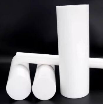
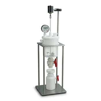
The Solution: Precision-Engineered PTFE and PFA
To achieve sub-PPB purity, you cannot rely on off-the-shelf components. You need a fluid path that is as sophisticated as the chip you are building. This is why Polytetrafluoroethylene (PTFE) and Perfluoroalkoxy (PFA) are the industry standards—but only when they are engineered with precision.
At KINTEK, we don't just provide "plastic parts." We design and CNC-fabricate high-purity PTFE and PFA components specifically to address the root causes of contamination:
- Ultra-Low Extractables: Our high-purity PFA labware and fluid components are selected for their total chemical inertness, ensuring that no ionic or organic contaminants migrate into your specialty gases or deionized water.
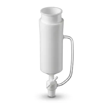
- Advanced Surface Smoothing: Through custom CNC fabrication, we ensure that the internal surfaces of our valves and fittings are incredibly smooth. This reduces particle entrapment and prevents the "non-stick" nature of PTFE from being compromised by microscopic burrs or rough patches.
- Eliminating Dead-Legs: Our custom-designed fluid transfer components are engineered to eliminate stagnant zones. This ensures a "first-in, first-out" fluid flow, which is essential for managing ultrapure etchants and stripping solutions in vapor-recovery condensers.
Beyond the Fix: Unlocking New Potential
When you solve the problem of fluid path contamination, you aren't just "fixing a leak"—you are expanding what your facility is capable of.
With a truly pure distribution system, you can move from "fighting fires" to "optimizing processes." You can achieve the stable, repeatable yields necessary for the next generation of smaller, faster semiconductors. You can run longer service cycles on your etching and wafer fabrication tools without fear of degradation or particle spikes.
By understanding the physics of the fluid path, you turn your distribution system from a liability into a strategic advantage.
Contamination control at the PPT level requires more than just the right material; it requires a partner who understands the rigorous demands of the semiconductor environment. Whether you are scaling a new energy project or refining a chemical research process, our team specializes in translating complex purity requirements into high-precision reality. Contact Our Experts today to discuss how our custom CNC PTFE and PFA solutions can safeguard your next breakthrough.
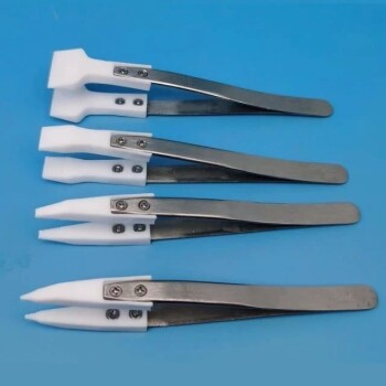
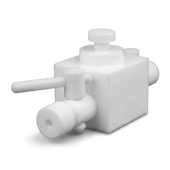
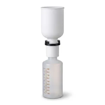
Related Products
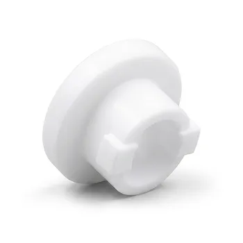
- Custom PTFE Insulating Gaskets Corrosion Resistant Teflon Seals Tailored Engineering Plastic Components
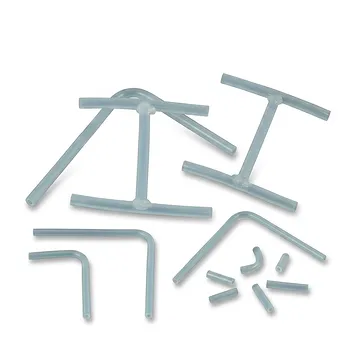
- High Performance PFA Coiled Spring Tubing and Custom PTFE Fabrication Services with Welded Fittings and Precision Bent Components
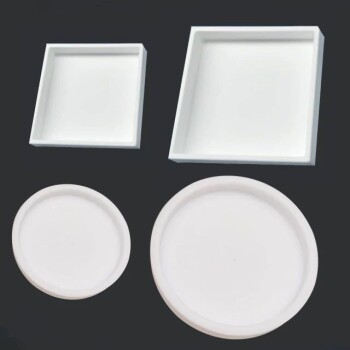
- Custom PTFE Parts Manufacturer for Teflon Containers and Components
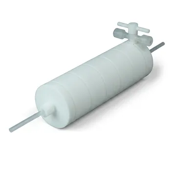
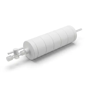
- High Purity PTFE Filter with PFA Valve Connections and Integrated Sieve Plate for Corrosive Fluid Processing
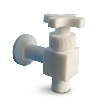
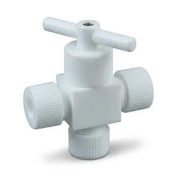
- Corrosion Resistant PTFE Polytetrafluoroethylene Valve and Customizable Laboratory Fluid Dispensing Faucet for Aggressive Chemical Handling in Industrial Storage Tanks and Plastic Drums
Related Articles
- Why 'Medical-Grade' Isn't Enough: The Hidden Risk in Your PTFE Components
- Beyond the Coating: The Physics of a Perfect Pitch and the Role of PTFE Components
- Beyond "Non-Stick": Why Your PTFE Components Fail and How to Fix It for Good
- The Asymmetric Cost of Failure: Why Precision PTFE Is Your Last Line of Defense
- The Silent Thief: How Component Surfaces Dictate Pharmaceutical Profitability