The Invisible Barrier to Perfect Yields
In the world of flat-panel display (FPD) manufacturing—whether you are producing OLEDs for smartphones or high-resolution LCDs for medical monitors—the margin for error is shrinking to the atomic level. You’ve likely seen it: a batch of ITO (Indium Tin Oxide) coated glass passes through a rigorous multi-stage cleaning line, only to emerge with "ghost" stains, localized refractive-index shifts, or microscopic metallic contamination that kills the final product's performance.
When these defects occur, most process engineers look at the chemical concentration of the bath or the purity of the deionized water. But the true culprit is often hiding in plain sight: the carrier holding the substrate.
The Cost of "Good Enough" Carriers
A common struggle in wet chemical processing (etching, developing, and stripping) is the reliance on generic carriers. Many labs and production facilities attempt to use standard plastic racks or lower-grade fluoropolymer containers that aren't designed for the extreme demands of modern electronics.
The consequences are not just technical; they are financial.
- Trace Contamination: Standard materials can leach ions or outgas, leading to metallic contamination. In 300mm wafer processing, even levels above 10 parts per trillion (ppt) can be catastrophic.
- Fluid Stagnation: If a basket isn’t designed for flow, "dead zones" trap spent chemicals or dislodged photoresist against the glass surface, resulting in uneven etching or staining.
- Yield Instability: When the carrier reacts—even slightly—with aggressive SC-1, SC-2, or HF-based baths, the process window shifts, making it impossible to achieve the repeatable results required for high-volume manufacturing.
The Root Cause: Why Material and Geometry Matter
To understand why these failures happen, we must look at the underlying science of the interface between the substrate and the carrier.
In flat-panel manufacturing, you are often dealing with ITO or FTO conductive glass. These surfaces are incredibly sensitive to their environment. A "standard" plastic carrier can introduce two critical failure points. First is ion leaching: low-purity materials release contaminants that chemically bond to the transparent conductive oxide (TCO) layer, permanently altering its optical properties. Second is refractive index interference: if the basket material interacts with the cleaning solution, it can leave a microscopic residue that changes how light passes through the glass.
True success isn't just about "not melting" in acid; it’s about being chemically neutral. This is where high-purity Polytetrafluoroethylene (PTFE) becomes essential. Because it is totally inert and has a high-purity material profile with virtually zero extractables, it ensures that the only reaction happening in the tank is the one you intended.
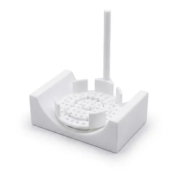
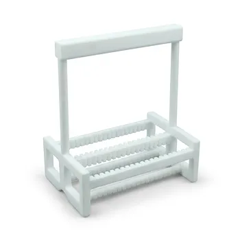
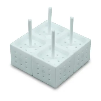
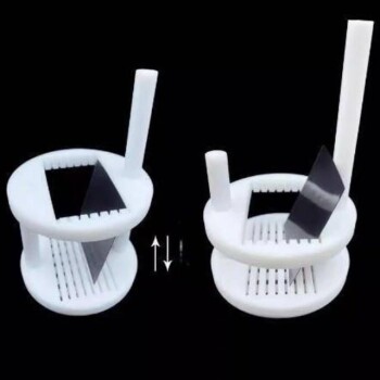
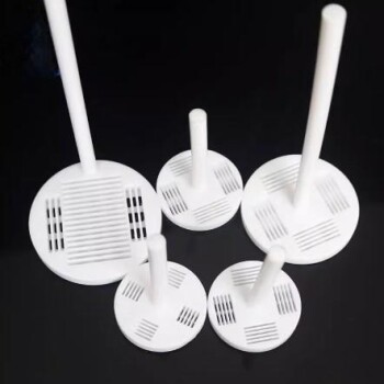
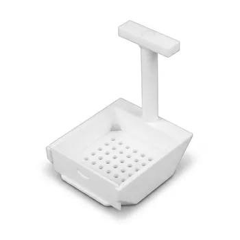
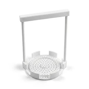
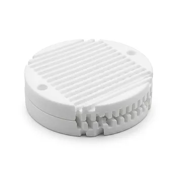
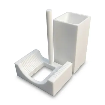
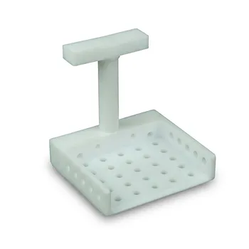
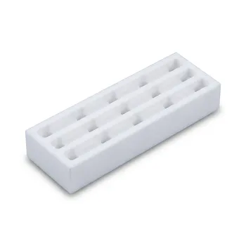
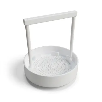
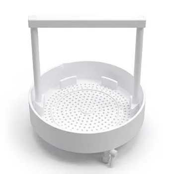
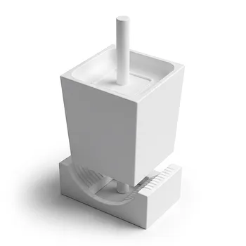
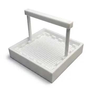
The Solution: Precision-Engineered PTFE Flower Baskets
Solving the problem of substrate contamination requires more than just a different material—it requires a tool designed as a piece of high-precision laboratory equipment. This is where the PTFE Flower Basket (also known as a wafer cleaning rack) changes the equation.
At KINTEK, our PTFE flower baskets are not just "holders." They are engineered solutions based on deep material science:
- Total Chemical Inertness: Using high-purity PTFE ensures that during RCA cleaning or HF etching, there is no particle generation and no ion leaching.
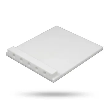
- Optimized Fluid Dynamics: Through custom CNC fabrication, our baskets feature slotted and perforated designs that maximize fluid flow. This ensures that cleaning, rinsing, and drying agents contact the substrate uniformly and drain completely, preventing the "edge effects" that ruin display panels.
- Thermal Stability: These baskets maintain their structural integrity across extreme temperature ranges, preventing the substrate from shifting or cracking during high-temperature stripping or developing phases.
By choosing a tool fabricated specifically for your substrate’s dimensions, you move from "managing defects" to "preventing them by design."
Beyond the Fix: Unlocking New Production Potential
When you resolve the fundamental issue of carrier-induced contamination, the benefits ripple across your entire production line.
With a stable, high-purity carrier system, you can finally push the boundaries of your process. This means successfully cleaning thinner, more delicate flexible substrates without fear of breakage. It means achieving the sub-10 ppt purity levels required for the next generation of semiconductor and display technologies. Most importantly, it means a dramatic increase in your yield-per-batch, reducing the massive costs associated with scrap and project delays.
A PTFE flower basket might seem like a simple component, but it is the silent guardian of your most sensitive processes. When the "invisible" physics of your carrier works with you instead of against you, the path to a flawless finish becomes clear.
Choosing the right equipment is the first step toward optimizing your wet chemical processing and protecting your high-value substrates. Whether you are scaling an industrial display line or conducting trace analysis in a specialized lab, our team can provide the custom-fabricated PTFE and PFA solutions your project demands. To discuss your specific substrate dimensions or chemical compatibility requirements, don't hesitate to reach out. Contact Our Experts to start engineering your path to higher yields.
Related Products
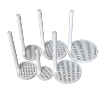
- High Purity PTFE Wet Cleaning Flower Basket Single Wafer Etching Rack Customizable 4 Inch Mask Plate Carrier
- PTFE Polytetrafluoroethylene Flower Basket Small Silicon Wafer Cleaning Rack Carrier for Laboratory Acid Pickling
- Custom PTFE Wafer Cleaning Flower Basket Chemical Resistant Fluoropolymer Carrier for Semiconductor Etching and New Energy Processing
- Custom PTFE Teflon Parts Manufacturer Adjustable Height Flower Basket
- Custom Machined Molded PTFE Teflon Parts Manufacturer for Laboratory ITO FTO Conductive Glass Cleaning Flower Basket