The High-Stakes Challenge of "Un-Bondable" Microfluidics
You have spent weeks designing a microfluidic reactor for a highly corrosive chemical synthesis. You choose Polytetrafluoroethylene (PTFE) because nothing else survives the pH levels and temperatures of your experiment. But when the chip finally arrives and you start the pump, the reality sets in: the channels are slightly distorted, or worse, the fluid is weeping from the edges of the bond.
In the world of microfluidics, PTFE is both a dream material and a fabrication nightmare. Its "non-stick" nature, which makes it so valuable for chemical purity, also makes it notoriously difficult to assemble into a leak-proof, planar chip. If you have ever faced inconsistent flow rates or contaminated samples due to failing seals, you are not alone.
The Common Struggle: Why Standard Methods Fall Short
When researchers or engineers first attempt to build PTFE microfluidic devices, they often run into a wall. Standard plastic fabrication techniques simply don't work.
- The Bonding Failure: You cannot use traditional adhesives or glues because PTFE’s surface energy is too low—nothing sticks to it. Furthermore, any glue you could use would likely dissolve and contaminate your ultra-pure chemical reaction.
- The Molding Myth: Unlike standard thermoplastics like Polypropylene, you cannot simply injection-mold PTFE into a complex micro-cavity.
- The Leakage Trap: Many resort to simple mechanical clamping. However, because PTFE is prone to "cold flow" (it deforms slowly under constant pressure), a seal that is tight on Monday might be leaking by Wednesday.
These failures aren't just technical hiccups; they result in expensive project delays, wasted high-purity reagents, and data that simply cannot be trusted.
The Root of the Problem: PTFE’s Unique "Non-Melting" Nature
To solve these issues, we must understand the underlying physics of the material. Unlike most plastics, PTFE has an extremely high melt viscosity. Even when heated to its transition point (around 327°C), it does not flow like a liquid; it becomes a rubbery gel.
This is why traditional bonding fails. Most microfluidic chips are made by melting two surfaces together. With PTFE, if you don't reach exactly the right temperature—typically between 360°C and 380°C—the polymer chains will never fuse.
Furthermore, because it is a soft material, "cutting" a microchannel isn't as simple as it looks. Standard tools can cause the material to "smear," resulting in channels that aren't square or dimensions that drift. This lack of precision at the micron level is the primary cause of sealing failures; if the surface isn't perfectly flat, no amount of pressure will create a hermetic seal.
The Solution: A Two-Pronged Approach to Precision
Truly reliable PTFE microfluidic chips require a departure from "standard" plastic shop practices. At KINTEK, we address the root cause through a combination of precision machining and specialized bonding:
1. High-Precision CNC Machining
Because PTFE cannot be molded into complex shapes, it must be carved. We utilize precision CNC milling and turning to create microchannels directly into technical-grade PTFE blocks. This allows for custom geometries that are far more complex than what molding can achieve, while maintaining the structural integrity of the material.
2. Advanced Sealing Architectures
To solve the bonding crisis, we utilize two primary methods:
- Thermal Bonding with FEP Interlayers: We use a thin layer of FEP (Fluorinated Ethylene Propylene) as a "bonding agent." FEP has a lower melting point than PTFE, allowing it to act as a high-performance, chemically resistant "hot melt" that fuses the PTFE plates together without deforming the microchannels.
- Mechanical 'Click' Systems: For chips that need to be cleaned or reconfigured, we engineer tenon-and-mortise interlocking systems. These "click" together under compression, using the material's own geometry to create a high-pressure seal that resists the effects of cold flow.
Beyond the Fix: Unlocking New Chemical Frontiers
When you solve the problem of the "un-bondable" chip, you open doors to research that was previously impossible. With a perfectly sealed, high-precision PTFE chip, you can move beyond simple flow observations.
Imagine running continuous-flow synthesis of aggressive reagents for weeks at a time without a single drop of leakage. Consider the ability to perform trace analysis in the semiconductor or new energy sectors, knowing that your labware is contributing zero contaminants to the sample. By mastering the fabrication of PTFE, we transform it from a "difficult material" into a reliable platform for the next generation of chemical and battery research.
The challenges of microfluidic fabrication shouldn't be the bottleneck in your research. At KINTEK, we combine deep material science with end-to-end CNC expertise to turn your most complex designs into high-performance reality. Whether you are prototyping a single reactor or scaling up to industrial volumes, our team is ready to help you overcome the "PTFE hurdle" and achieve the precision your work demands. Contact Our Experts to discuss your project requirements today.
Related Products
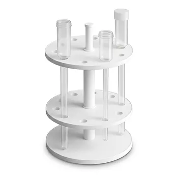
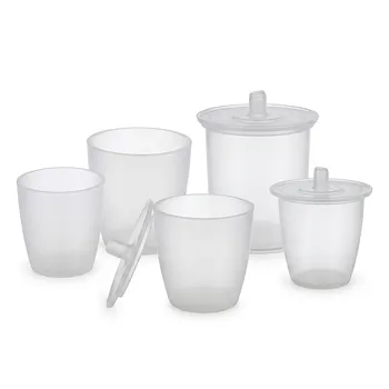
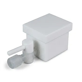
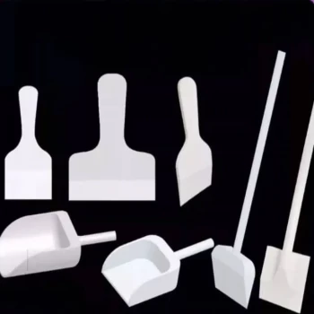
- Custom PFA Micro Column Rack and PTFE Machined Storage Solutions for Trace Analysis
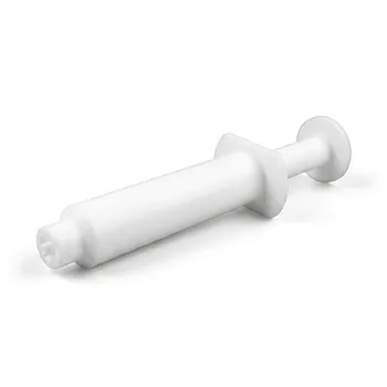
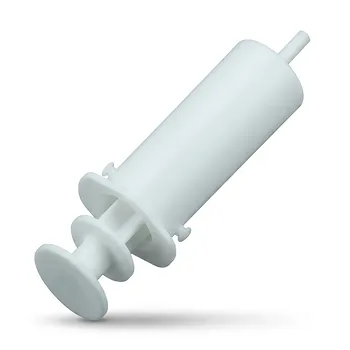
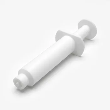
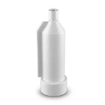
- High Purity 25ml PTFE Syringe for Trace Analysis and Automated Syringe Pump Systems
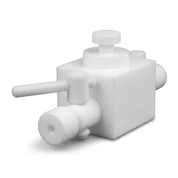
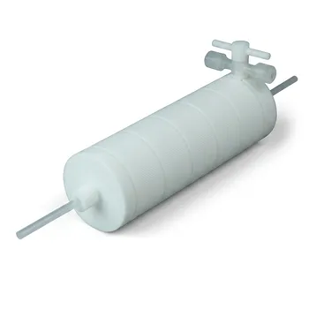
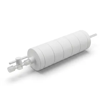
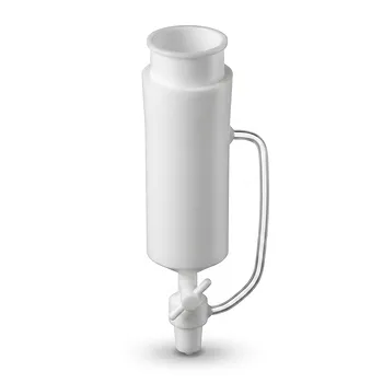
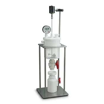
- Custom PTFE Filtration System Acid Resistant High Purity Semiconductor Grade Chemical Processing Filter
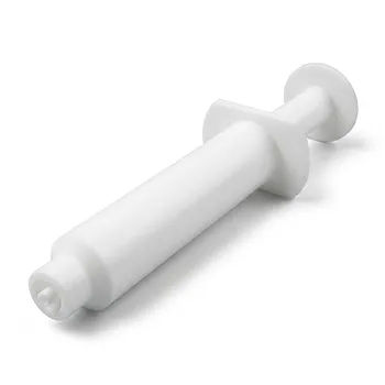
- Virgin PTFE Precision Syringe for Chemical Dispensing and Syringe Pump Integration with FEP Tubing Compatibility
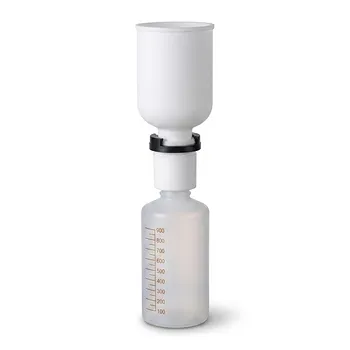
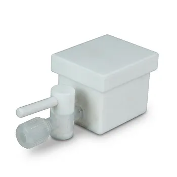
- PTFE PFA Vacuum Filtration System Corrosion Resistant Customizable Shatterproof Laboratory Device