PTFE(Teflon) Labware
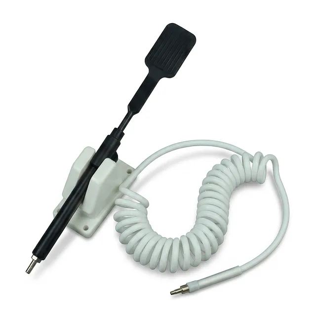
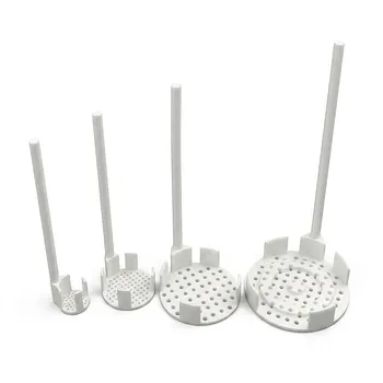
High Precision ESD Safe PEEK Wafer Vacuum Suction Pen for 8 Inch Semiconductor and Photovoltaic Substrate Handling
Item Number : PL-CP115
Price varies based on specs and customizations
- Primary Construction Material
- ESD-Safe PEEK (Polyetheretherketone)
- Substrate Compatibility
- Fully Customizable for 8-Inch Wafers and Special Substrates
- Manufacturing Process
- End-to-End Custom CNC Fabrication
Shipping:
Contact us to get shipping details Enjoy On-time Dispatch Guarantee.
Why Choose Us
Easy ordering process, quality products, and dedicated support for your business success.
Product Overview
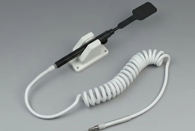
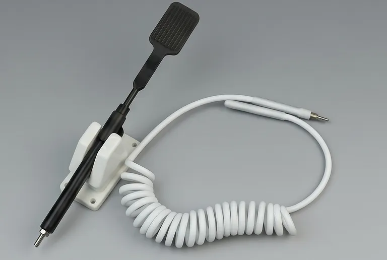
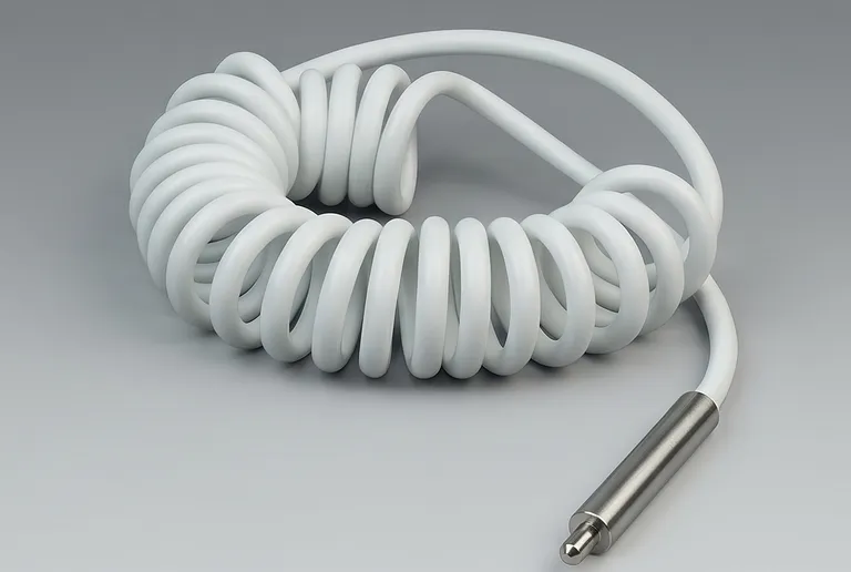
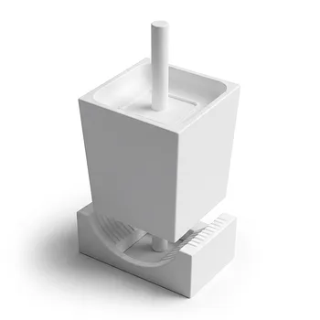
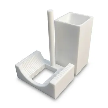
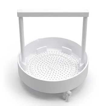
This high-performance manual handling system is engineered for the delicate manipulation of 8-inch wafers and sensitive substrates within the semiconductor and photovoltaic industries. Developed to bridge the gap between automated transport and manual intervention, this unit provides an ultra-secure vacuum grip that minimizes physical contact while maximizing stability. By utilizing high-grade PEEK (Polyetheretherketone) material, the tool ensures that fragile wafers are protected from mechanical stress, surface contamination, and electrostatic discharge during critical inspection or transfer phases.
Designed specifically for rigorous cleanroom environments, the equipment excels in scenarios where standard handling tools fail due to material degradation or static buildup. It is an essential component for technicians and engineers working in wafer fabrication, solar cell assembly, and advanced R&D labs. The integration of advanced ESD-safe properties ensures that sensitive microelectronics are shielded from the catastrophic effects of electrostatic discharge, maintaining the integrity of high-value components throughout the manufacturing cycle.
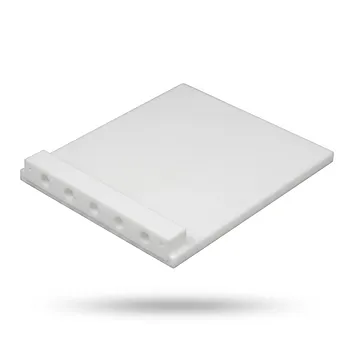
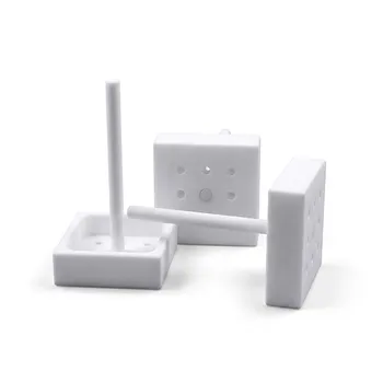
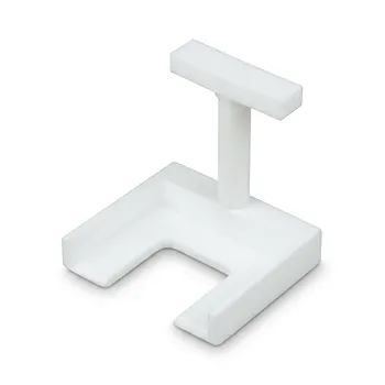
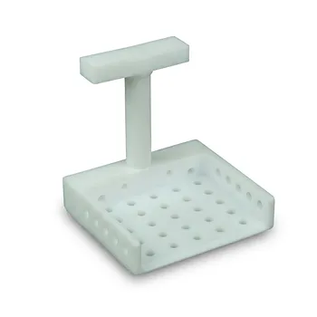
With a focus on long-term reliability and operational consistency, this system is built to withstand repeated exposure to various process chemicals and high temperatures without compromising its structural integrity. The precision-machined interface and ergonomic handle allow for fatigue-free operation over extended shifts, ensuring that delicate handling tasks are performed with the highest degree of accuracy. Every unit is treated as a bespoke engineering project, designed to meet the exact vacuum and dimensional requirements of specialized industrial workflows.
Key Features
- Advanced ESD-Safe PEEK Construction: The main body and contact tips are fabricated from premium ESD-safe PEEK, providing permanent static dissipative properties that protect sensitive circuits from electrostatic damage during handling.
- Superior Chemical Resistance: This material choice ensures the system remains inert and durable even when exposed to aggressive acids, bases, and organic solvents commonly found in semiconductor cleaning and etching processes.
- High-Temperature Thermal Stability: The unit maintains its mechanical strength and dimensional precision in high-heat environments, allowing for the safe handling of wafers directly from thermal processing stages.
- Non-Marring Contact Surface: The vacuum tip is precision-engineered to provide a secure seal without leaving residues, scratches, or particulate contamination on the 8-inch wafer surface.
- Ergonomic Handheld Architecture: The handle is designed with an emphasis on operator comfort and control, featuring a balanced center of gravity to reduce manual fatigue during high-volume wafer sorting.
- Efficient Vacuum Control Mechanism: A responsive vacuum trigger or button allows for instantaneous pickup and release, providing the operator with tactile feedback and total control over the substrate.
- Ultra-Low Outgassing Profile: Suitable for high-vacuum and ultra-clean environments, the materials used in this system minimize molecular contamination, ensuring compatibility with ISO Class 3 and above cleanrooms.
- Customizable Interface Geometry: The suction interface can be tailored to match specific wafer thicknesses, edge profiles, or surface textures, ensuring a perfect vacuum seal for non-standard substrates.
- Wear-Resistant Longevity: Unlike standard plastics, the high-performance fluoropolymer and PEEK components offer exceptional wear resistance, significantly extending the service life of the tool in 24/7 industrial production lines.
- Bespoke CNC Precision: Every component is manufactured using high-end CNC machining techniques, allowing for tighter tolerances and more complex geometries than standard molded alternatives.
Applications
| Application | Description | Key Benefit |
|---|---|---|
| Wafer Inspection | Manual transfer of 8-inch silicon wafers to and from optical or SEM inspection stations. | Minimal contact area reduces risk of surface defect generation. |
| Photovoltaic Cell Sorting | Handling and sorting of high-efficiency solar cells during the assembly and testing phases. | Prevents micro-cracks and maintains cell efficiency through gentle vacuum grip. |
| Wet Bench Processing | Transferring substrates between chemical baths or rinsing stations in wet chemistry environments. | Outstanding resistance to harsh process chemicals and moisture. |
| Thin-Film Deposition | Placing and removing substrates from PVD/CVD vacuum chambers or load locks. | High thermal stability allows for handling after high-temperature deposition cycles. |
| Cleanroom R&D | General substrate handling in advanced materials research and development facilities. | Maintains strict ISO cleanliness standards by minimizing particulate shedding. |
| Die Bonding Prep | Manual positioning of wafers for dicing or subsequent die bonding operations. | ESD-safe properties prevent latent defects in sensitive micro-circuits. |
| LED Substrate Handling | Precision manipulation of sapphire or SiC substrates during LED chip manufacturing. | Secure grip on hard, polished surfaces without slippage or scratching. |
Technical Specifications
| Specification Category | PL-CP115 Specification Detail |
|---|---|
| Model Identification | PL-CP115 Series |
| Primary Material | High-Performance ESD-Safe PEEK |
| Substrate Compatibility | Fully Customizable (Optimized for 8-inch/200mm wafers) |
| Surface Resistance | Customizable to specified ESD-safe ranges (e.g., 10^6 - 10^9 Ω) |
| Operating Temperature Range | Customized based on process requirements |
| Chemical Compatibility | Universal (Highly resistant to most acids, bases, and solvents) |
| Vacuum Connection Type | Bespoke sizing to match facility vacuum lines or portable pumps |
| Tip Configuration | Custom shapes (flat, curved, multi-point) available upon request |
| Cleanroom Rating | Compatible with ISO Class 3 - 8 (Application dependent) |
| Manufacturing Method | Precision CNC Machined to Bespoke Specifications |
| Handle Dimensions | Ergonomically tailored to client preferences |
Why Choose High Precision ESD Safe PEEK Wafer Vacuum Suction Pen for 8 Inch Semiconductor and Photovoltaic Substrate Handling
- Precision Engineered Reliability: This system is not a mass-produced commodity but a precision-machined instrument designed for the world's most demanding cleanroom environments. Its robust construction ensures that it performs consistently under heavy industrial use without the material degradation typical of standard handling tools.
- Bespoke Material Performance: By leveraging the unique properties of ESD-safe PEEK, we provide a tool that is simultaneously lightweight, chemically inert, and thermally stable. This material advantage directly translates to higher yields and lower risk of wafer breakage or contamination.
- Total Customization Capability: We understand that every fabrication line has unique requirements. Whether you need a specific vacuum tip geometry, a particular surface resistance level, or a custom handle length, our engineering team can adapt the design to fit your exact operational parameters.
- Operational Continuity: Investing in high-quality fluoropolymer and PEEK tools reduces the frequency of replacements and the risk of unexpected failures. This reliability is crucial for maintaining throughput in high-value semiconductor and photovoltaic production lines.
- Cleanroom Integrity: Every component is designed with contamination control as a priority. From the low-particulate shedding of the PEEK material to the easy-to-clean smooth surfaces, this equipment supports your efforts to maintain the strictest environmental standards.
For technical consultations or to request a quote for a custom-configured handling solution tailored to your specific process requirements, please contact our engineering department today.
Trusted by Industry Leaders
REQUEST A QUOTE
Our professional team will reply to you within one business day. Please feel free to contact us!
Related Products
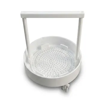
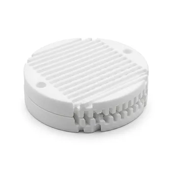
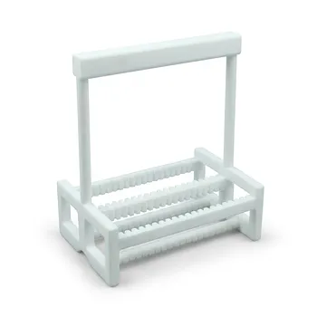
Semiconductor PTFE Wafer Carrier 8 Inch Wet Cleaning HF Resistant Etching Cassette
Optimize semiconductor processing with this premium PTFE 8 inch wafer carrier designed for high-purity wet cleaning and HF etching applications. Our industrial-grade fluoropolymer cassettes ensure maximum chemical resistance, superior durability, and precise handling for sensitive cleanroom production environments.
PTFE Silicon Wafer Holder for Acid Etching and Cleaning Process 2 4 6 8 Inch Customizable High Temperature Resistant
High-purity PTFE silicon wafer holders engineered for extreme acid etching and cleaning processes. Optimized for 2 to 8 inch wafers, these robust customizable carriers ensure contamination-free handling and thermal stability in the most demanding semiconductor fabrication environments for B2B procurement.
High Purity PTFE Wafer Cassette Etching Carrier for Semiconductor Silicon Wafer Cleaning and Acid Resistance
Premium PTFE wafer cassettes engineered for semiconductor etching and cleaning. Superior HF resistance and high-purity construction ensure safe silicon wafer handling in critical wet processes. Ideal for 2-inch to 12-inch substrates in cleanroom environments.
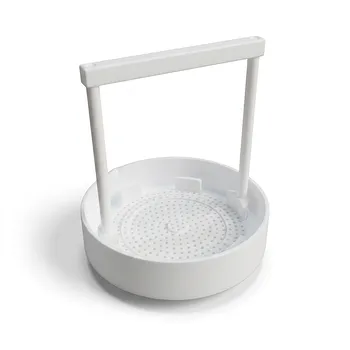
PTFE Circular Wafer Carrier 6 Inch Acid Alkali Resistant Semiconductor Cleaning Basket Customizable
High-purity 6-inch PTFE circular wafer carriers designed for semiconductor cleaning. Excellent acid and alkali resistance for piranha and HF etching. Precision-machined, fully customizable baskets ensure safe substrate handling during demanding wet chemical processes, immersion baths, and ultrasonic rinsing.
6 Inch Circular PTFE Wafer Carrier Acid and Alkali Resistant Semiconductor Cleaning Flower Basket Customizable
High-purity 6-inch PTFE wafer carriers designed for critical semiconductor wet processing. Engineered for extreme chemical resistance and thermal stability, these customizable flower baskets ensure uniform cleaning and substrate protection in harsh acidic and alkaline immersion environments throughout production.
Custom PTFE Wafer Cleaning Baskets Semiconductor Silicon Wafer Holders Low Background Fluoropolymer Cassettes
High-purity custom PTFE wafer cleaning baskets for semiconductor processing. Engineered for low background trace analysis and aggressive chemical resistance, these bespoke fluoropolymer cassettes ensure zero dissolution and contamination-free handling of silicon wafers in critical cleanroom environments and industrial laboratories.
Custom PTFE Wafer Carrier Flower Basket Chemical Resistant Semiconductor Cleaning Handle Design
Maximize semiconductor yield with custom PTFE wafer carriers and flower baskets. Designed for superior resistance to hydrofluoric acid and harsh reagents, these high-purity handling systems feature ergonomic handles and precision CNC-machined slots for secure, contamination-free wet process cleaning.
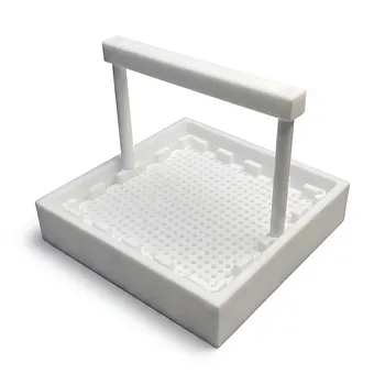
Customizable Square PTFE Silicon Wafer Cleaning Flower Basket for Semiconductor Wet Process Etching and Substrate Handling
High-purity PTFE square cleaning flower baskets designed for silicon wafer processing. This corrosion-resistant rack ensures safe wet etching and substrate handling in semiconductor manufacturing. Fully customizable dimensions and configurations are available to meet specific laboratory or industrial wet bench requirements.
Custom PTFE Wafer Cleaning Flower Basket Chemical Resistant Fluoropolymer Carrier for Semiconductor Etching and New Energy Processing
Optimize your semiconductor and new energy manufacturing with custom PTFE wafer cleaning flower baskets. Engineered for extreme chemical resistance during etching and RCA cleaning, these high-purity fluoropolymer carriers ensure process integrity and long-term durability in demanding industrial environments.
Square PTFE Wafer Cleaning Basket Fluoropolymer Semiconductor Etching Rack Custom Silicon Wafer Carrier
Optimize semiconductor wet bench processes with our custom square PTFE wafer cleaning baskets. Engineered for extreme chemical resistance and high-purity handling, these fluoropolymer carriers offer superior durability and precision for critical silicon wafer etching and cleaning.
Semiconductor PTFE Cleaning Basket 12 Inch Wafer Wet Etching Rack Acid Alkali Resistant Fluoropolymer Carrier
Engineered for high-purity semiconductor environments, this 12-inch PTFE wafer cleaning basket ensures exceptional chemical resistance during critical wet etching and cleaning processes. The custom-fabricated design provides reliable wafer support and maximum fluid exposure for precision manufacturing.
High Purity PTFE Wafer Carrier Semiconductor Flower Basket for Corrosion Resistant Silicon Processing Custom Sized Labware
Optimize semiconductor cleaning with our high purity PTFE wafer carriers featuring extreme chemical resistance and fully customizable dimensions for precision silicon processing workflows including RCA clean and piranha etching procedures in advanced cleanroom environments today.
Custom PTFE Semiconductor Wafer Cleaning Basket Corrosion Resistant Low Background Lab Rack
Achieve superior purity in semiconductor manufacturing with our custom PTFE cleaning baskets. Engineered for extreme chemical resistance and low background interference, these durable racks ensure efficient wafer processing, rapid drainage, and reliable performance in critical high-purity laboratory environments.
Custom PTFE Wafer Carrier Cleaning Basket Corrosion Resistant Non Leaching High Polymer Experiment Support
High-performance custom PTFE wafer carriers and cleaning baskets designed for semiconductor and polymer research. Featuring exceptional corrosion resistance and zero-leaching properties, these bespoke solutions ensure contamination-free processing in demanding chemical environments for high precision laboratory and industrial applications today.
PTFE Polytetrafluoroethylene Flower Basket Small Silicon Wafer Cleaning Rack Carrier for Laboratory Acid Pickling
This high-purity PTFE flower basket provides exceptional chemical resistance for silicon wafer cleaning and acid pickling. Designed for precision laboratory applications, it ensures uniform fluid penetration and contamination-free handling of delicate semiconductor substrates in harsh chemical environments.
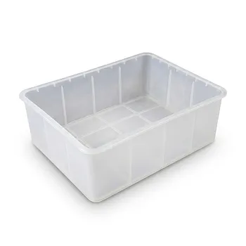
Laboratory PFA Rectangular Acid Soaking Tank Silicon Wafer Cleaning Bath Corrosion Resistant High Purity Vessel
High purity PFA rectangular tank engineered for semiconductor silicon wafer cleaning and corrosive acid soaking. This chemically inert laboratory vessel offers superior thermal stability and ultra low trace metal backgrounds for critical trace analysis and industrial cleaning processes.
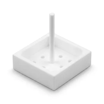
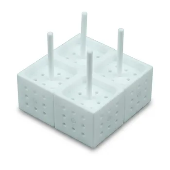
Custom PTFE Wafer Handling Rack Corrosion Resistant High Temperature Semiconductor Polysilicon Processing Stand
Premium custom PTFE wafer stands engineered for extreme chemical environments and high-temperature semiconductor processing. These corrosion-resistant carriers ensure high-purity handling, low-friction operation, and exceptional durability for critical polysilicon, photovoltaic, and advanced electronics manufacturing workflows.
PTFE Wafer Cleaning Basket 4 Inch Etching Rack Acid Alkali Resistant Custom Mask Carrier
Precision-engineered PTFE etching baskets designed for semiconductor wafer cleaning and chemical processing. These acid-resistant, high-purity cleaning racks ensure zero contamination in demanding laboratory environments. Fully customizable to meet specific industrial mask and wafer dimensions for advanced manufacturing and research applications.
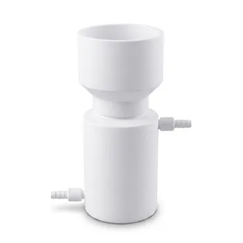
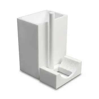
High Purity PTFE Buchner Funnel Vacuum Filtration System Corrosion Resistant Low Trace Laboratory Suction Filter Apparatus
Optimize your laboratory workflows with our premium PTFE Buchner funnel vacuum filtration systems. Engineered for extreme chemical resistance and low-trace analysis, these durable units provide reliable suction for demanding industrial and scientific sample preparation processes.
Custom PTFE Square Tank Semiconductor Soaking Cleaning Acid Resistant Fluoropolymer Filtration Vessel
Maximize efficiency in semiconductor fabrication with our custom PTFE square tanks, engineered for superior acid resistance and trace analysis purity. These high-performance fluoropolymer vessels ensure contaminant-free soaking and reliable chemical handling for demanding laboratory and industrial processes today.