The High Cost of "Microscopic" Failure
Imagine a semiconductor fabrication plant where a single batch of 300 mm wafers, worth hundreds of thousands of dollars, is suddenly flagged for defects. The culprit isn't a mechanical failure or a software glitch; it is a trace amount of metallic ions, measured in parts per trillion (ppt), that leached into the deionized water from a "standard" fluid line.
Similarly, in the food and beverage industry, a production run is discarded because the previous batch’s flavor profile "carried over" despite a rigorous cleaning cycle. These aren't just technical hiccups; they are significant commercial setbacks that lead to project delays, wasted materials, and compromised brand reputations. If your data or product quality feels like it's on a "rollercoaster" despite following every protocol, the problem likely isn't your process—it’s the material handling it.
The Common Struggle: Why Standard Solutions Fall Short
When faced with contamination, most engineering teams reach for the traditional "fixes." They might increase the frequency of Clean-in-Place (CIP) cycles, use more aggressive chemical etchants, or upgrade to stainless steel components.
However, these "solutions" often create a new set of headaches:
- The Corrosion Trap: Stainless steel, while durable, can still succumb to aggressive etchants like hydrofluoric acid (HF), leading to metallic ion leaching.
- The Porosity Problem: Many standard plastics have microscopic surface irregularities where bacteria can anchor or where "flavor ghosts" can hide, resisting even the most intense cleaning.
- Material Fatigue: Repeated exposure to harsh CIP chemicals or high-temperature steam causes many polymers to become brittle, leading to particle shedding—the ultimate enemy of the semiconductor cleanroom.
The Root Cause: It’s Not Just About the Surface
The reason these common struggles persist is that the "enemy" operates at a molecular level. Most materials interact with the fluids they carry. Whether it is ionic leaching (where the material "bleeds" atoms into the fluid) or low surface energy (where the fluid sticks to the material), the failure is baked into the material's chemistry.
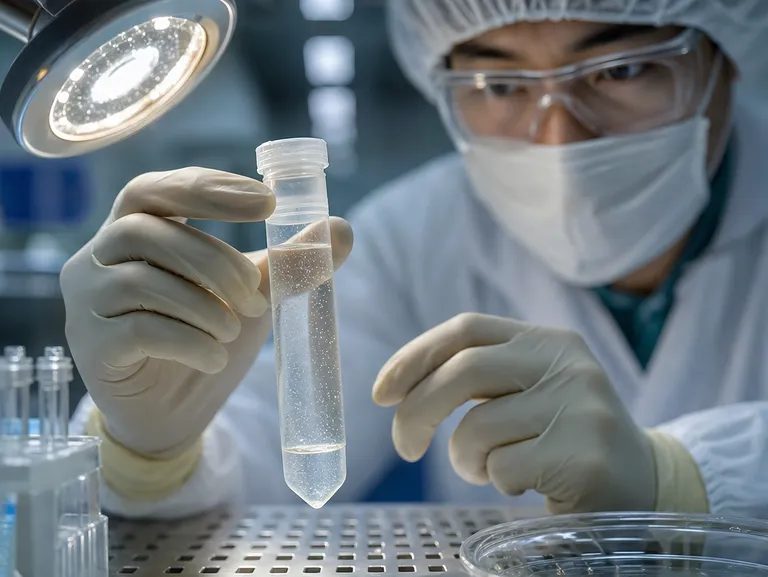
In semiconductor manufacturing, maintaining metallic contamination below 10 ppt is non-negotiable. Standard materials often fail here because they contain "extractables"—residual chemicals from the manufacturing process that outgas or leach into ultra-pure process gases and chemicals. When you use materials that aren't chemically inert, the "purity" of your input is irrelevant, because the delivery system itself is the source of the pollution.
The Solution: PTFE as an Engineered Purity Barrier
To solve the root cause of contamination, you need a material that is effectively "invisible" to the chemicals it touches. This is why Polytetrafluoroethylene (PTFE) and PFA have become the gold standard for high-stakes manufacturing.
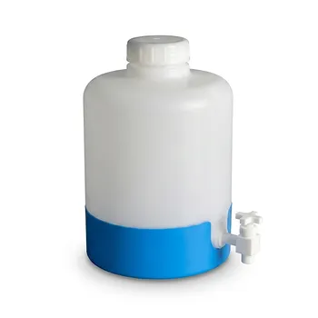
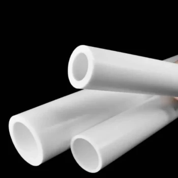
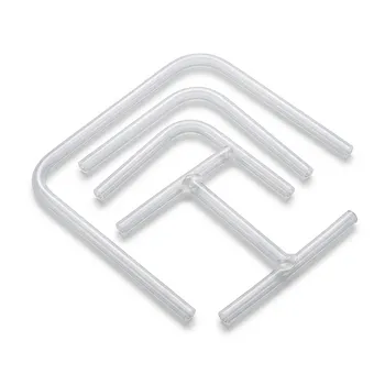
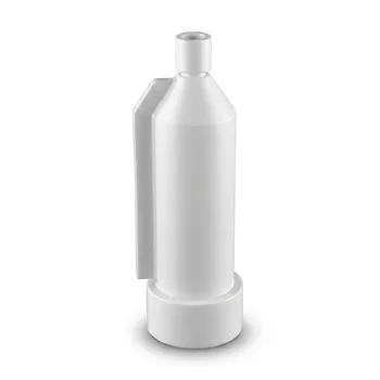
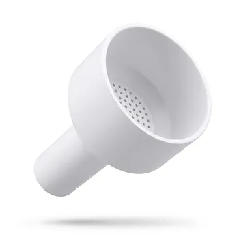
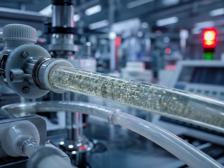
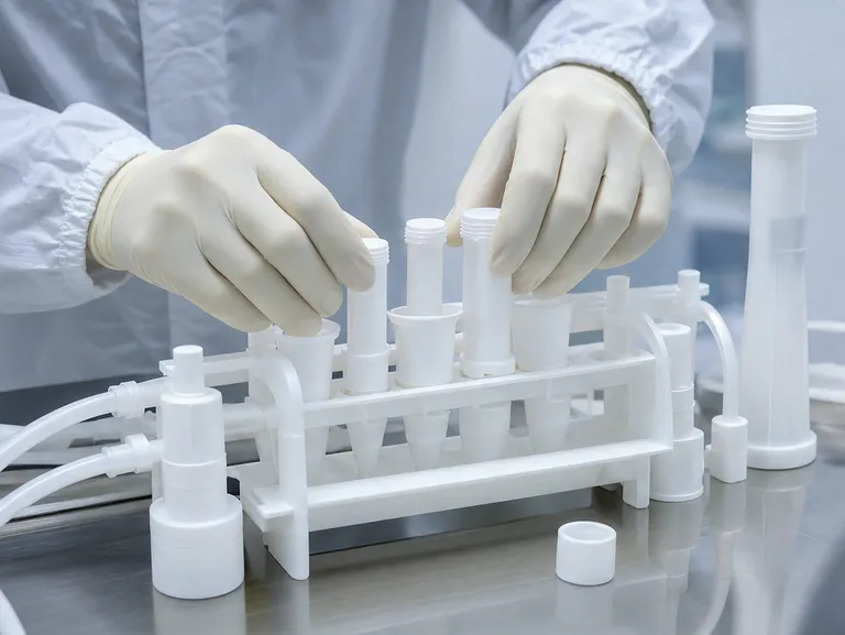
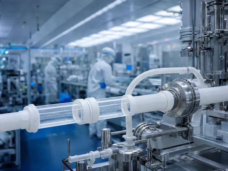
At KINTEK, we don't just view PTFE as a commodity; we treat it as a high-precision tool. Our PTFE and PFA products—from capillary tubing to custom-machined microwave digestion vessels—provide a solution rooted in three physical certainties:
- Total Chemical Inertness: PTFE does not react with aggressive etchants, peroxides, or solvents. It won't participate in catalytic side reactions or degrade when exposed to the harshest industrial chemicals.
- Zero-Retention Surfaces: The non-stick nature of PTFE means that residues from things like Chemical Mechanical Planarization (CMP) slurries or organic food dyes simply cannot adhere. This eliminates "carry-over" and makes CIP cycles significantly more effective.
- Ultra-Low Extractables: Our high-purity PFA and PTFE labware are designed to ensure that sub-ppb purity levels are maintained. There is no outgassing and no ion leaching, which is essential for protecting the yield of 300 mm wafers and sensitive trace analysis.
Beyond the Fix: Unlocking New Production Potentials
When you eliminate the "noise" of contamination, you do more than just solve a problem—you unlock new capabilities.
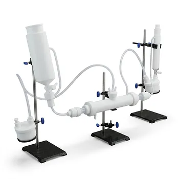
By moving to KINTEK’s high-precision PTFE fluid transfer components and custom CNC-fabricated parts, your facility can transition from "damage control" to "optimized output." You can run longer production cycles without fear of bacterial buildup. You can utilize more aggressive cleaning chemistries to ensure safety without worrying about damaging your equipment. In the semiconductor world, this means higher yields; in the chemical sector, it means more accurate, repeatable research data.
Precision is the difference between a successful batch and a costly error. Whether you are transporting ultra-pure specialty gases or designing a new hydrothermal synthesis process, the integrity of your material is the foundation of your success.
The challenges of contamination are complex, but the solution doesn't have to be. Our team at KINTEK specializes in translating these high-performance materials into the specific components—valves, fittings, and custom-machined fixtures—that your unique project demands. From specialized prototypes to high-volume industrial orders, we ensure that your fluid path is never the weak link in your process. Contact Our Experts today to discuss how we can help you achieve uncompromising purity in your next project.
Related Products
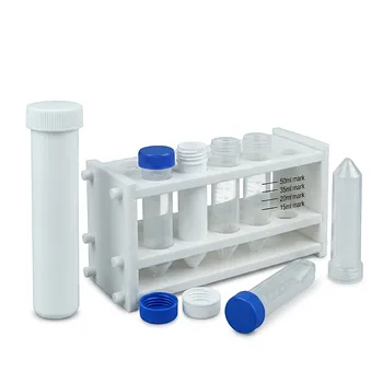
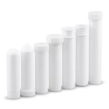
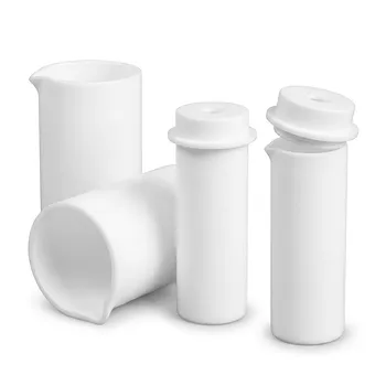
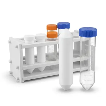
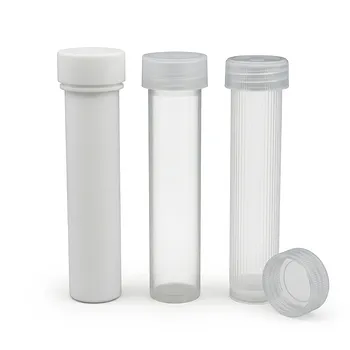
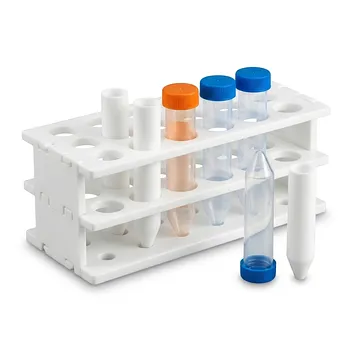
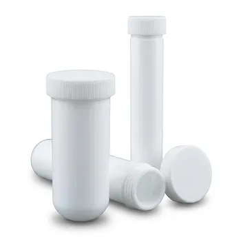
- Custom PTFE Digestion Tubes and High Purity Polytetrafluoroethylene Centrifuge Vessels 60ml for Trace Analysis
- Custom High Purity PTFE Digestion Tubes and Centrifuge Tubes for Trace Metal Analysis
- High Purity PTFE Digestion Tubes and Custom Centrifuge Tubes 100ml for Trace Analysis and Chemical Digestion
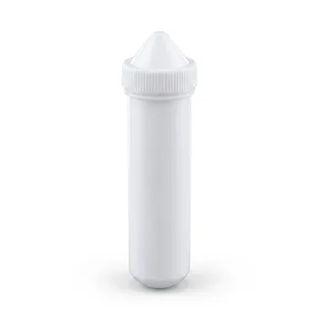
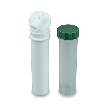
- Corrosion Resistant PTFE Digestion Tubes for Graphite Block Systems with Acid Reflux Caps Custom Dimensions
- High Purity PTFE Centrifuge Tubes for Trace Analysis Custom Laboratory Centrifugation Containers with Racks
Related Articles
- Beyond 'Non-Stick': The Physics and Psychology of Purity in PTFE Labware
- Why Your PTFE Labware Fails at High Temps—And It's Not the Bottle's Fault
- The Hidden Cost of Chemical Containers: Why Yours Are Failing and How to Fix It
- Beyond the Melting Point: Why Your PTFE Labware Fails Sooner Than You Think—And How to Fix It