In short, PTFE is used in the semiconductor industry because it possesses a rare combination of extreme chemical resistance, ultra-high purity, and excellent electrical properties. This makes it one of the few materials capable of withstanding the harsh manufacturing environment while preventing the microscopic contamination that can destroy a silicon wafer.
The core challenge in semiconductor fabrication is maintaining absolute purity in the presence of highly corrosive chemicals. PTFE is a cornerstone material because it is fundamentally non-reactive, ensuring that tools and components do not shed particles or react with process chemicals, thereby protecting device yield and performance.
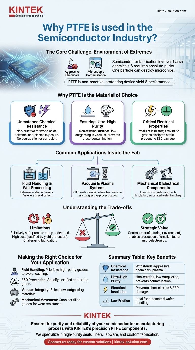
The Core Challenge: An Environment of Extremes
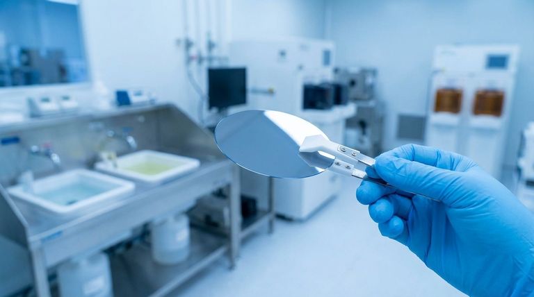
Semiconductor manufacturing is a battle fought on a microscopic scale. The process involves a sequence of aggressive chemical treatments, including the use of powerful acids and solvents during photolithography and etching.
At the same time, the environment must be kept immaculately clean. A single stray particle or a minute chemical impurity can create a defect that renders a multi-million dollar batch of microchips useless. Materials used in this environment cannot simply survive; they must perform without adding any contaminants.
Why PTFE Is the Material of Choice
PTFE (Polytetrafluoroethylene) meets these stringent demands through several key properties that make it uniquely suited for critical applications within a fabrication plant, or "fab."
Unmatched Chemical Resistance
The most critical property of PTFE is its near-total chemical inertness. It is non-reactive with the vast majority of industrial chemicals, including the strong acids and solvents used to etch silicon wafers.
This stability extends to plasma exposure, a common process in modern semiconductor manufacturing. Components made from PTFE will not degrade or corrode, ensuring the purity of the process chemistry.
Ensuring Ultra-High Purity
PTFE helps maintain the ultra-clean conditions required for high-yield chip production. Its surfaces are non-wetting, meaning liquids bead up and run off easily, simplifying the removal of chemical residues and preventing cross-contamination between process steps.
Furthermore, high-purity grades of PTFE exhibit very low outgassing characteristics. In the high-vacuum chambers used for deposition and etching, this means the material won't release trapped gases that could interfere with the process or contaminate the wafer surface.
Critical Electrical Properties
PTFE is an exceptional electrical insulator, which is vital for preventing short circuits in the complex wiring of manufacturing equipment. It is frequently used for cable insulation and connectors.
Crucially, PTFE is also available in anti-static grades. By adding specific fillers, the material can be made to safely dissipate static electricity, preventing electrostatic discharge (ESD) events that can instantly destroy sensitive electronic components during handling and processing.
Common Applications Inside the Fab
You will find PTFE in various forms throughout a semiconductor manufacturing facility, each leveraging its unique properties.
Fluid Handling and Wet Processing
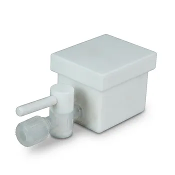
Because of its chemical resistance, PTFE is the standard material for custom labware, wafer containers, and wafer dippers used in "wet bench" processing, where wafers are submerged in acid baths. Fasteners and fittings made from PTFE ensure that even the smallest parts do not become a source of contamination.
Vacuum and Plasma Systems
In the high-vacuum chambers of etching and deposition tools, PTFE spring-energized seals are essential. They provide a reliable seal, resist aggressive process gases, and have the low outgassing properties necessary to maintain the ultra-clean vacuum environment.
Mechanical and Electrical Components
PTFE's low coefficient of friction makes it ideal for mechanical parts like guide rails and low-friction slide pads in automated wafer handling systems. Its insulative properties are used for high-performance cable insulation within the processing equipment itself.
Understanding the Trade-offs
While its benefits are clear, PTFE is not a universal solution. An objective assessment requires acknowledging its limitations.
Mechanical Strength
Standard PTFE is a relatively soft material and can be prone to "creep," or deformation under sustained load. It is not suitable for high-load structural applications unless it is reinforced with fillers, which can in turn impact its purity.
High Cost
High-purity, semiconductor-grade PTFE is significantly more expensive than most other polymers. However, this cost is easily justified when weighed against the catastrophic expense of a contaminated wafer batch, which can run into the millions of dollars.
Fabrication Complexity
Machining PTFE to the extremely tight tolerances required for semiconductor equipment can be challenging and requires specialized expertise and tools to maintain a smooth, particle-free finish.
Making the Right Choice for Your Application
Selecting the correct grade and form of PTFE is critical to leveraging its full potential in a semiconductor environment.
- If your primary focus is fluid handling: Prioritize high-purity grades of PTFE with documented resistance to your specific process chemicals to avoid leaching and contamination.
- If your primary focus is preventing ESD damage: Ensure you specify a certified anti-static grade for any components that will come near sensitive devices.
- If your primary focus is vacuum integrity: Select materials and seals with certified low-outgassing characteristics to protect deposition and etching processes.
- If your primary focus is mechanical movement: Consider filled grades of PTFE to improve wear resistance and reduce creep in parts like bearings or slide pads, while carefully vetting the filler material for purity.
Ultimately, using PTFE is a strategic decision to control the manufacturing environment, directly enabling the production of smaller, faster, and more reliable microelectronics.
Summary Table:
| Property | Benefit in Semiconductor Manufacturing |
|---|---|
| Chemical Resistance | Withstands aggressive acids, solvents, and plasmas without reacting or degrading. |
| Ultra-High Purity | Non-wetting surface and low outgassing prevent contamination of sensitive wafers. |
| Electrical Insulation | Excellent insulator; anti-static grades prevent electrostatic discharge (ESD) damage. |
| Low Friction | Ideal for mechanical parts in automated wafer handling systems. |
Ensure the purity and reliability of your semiconductor manufacturing process with KINTEK's precision PTFE components.
We specialize in manufacturing high-purity PTFE seals, liners, labware, and custom components for the semiconductor, medical, and laboratory industries. Our expertise in custom fabrication—from prototypes to high-volume orders—ensures you get parts that meet the extreme demands of your fab environment, protecting your yield and performance.
Contact us today to discuss your specific application and receive a quote for components built to your exact specifications.
Visual Guide
Related Products
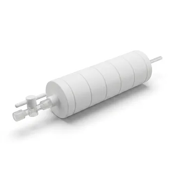
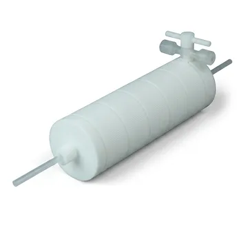
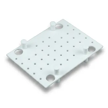
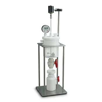
- Custom PTFE Filtration System Acid Resistant High Purity Semiconductor Grade Chemical Processing Filter
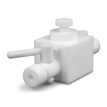
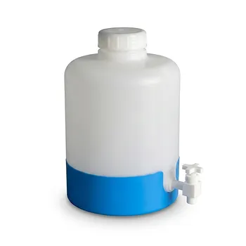
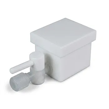
- High Corrosion Resistant PTFE Faucet Polytetrafluoroethylene Valve for Chemical Storage Drums and Fluid Transfer Systems Customizable Industrial Grade
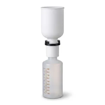
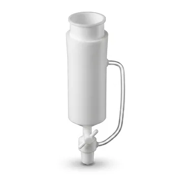
- PTFE PFA Vacuum Filtration System Corrosion Resistant Customizable Shatterproof Laboratory Device
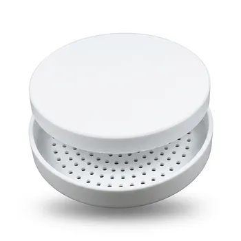
- PTFE Corrosion Resistant Filter with PFA Valve Connections and Integrated Sieve Plate
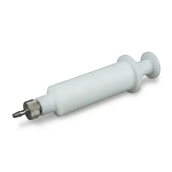
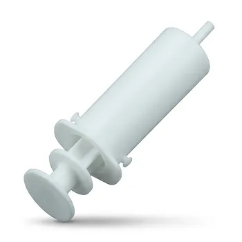
- High Temperature Chemical Resistant 50ml PTFE Syringe Customized Teflon Injector with Threaded Seal for Trace Analysis
People Also Ask
- What are common industrial applications of PTFE filters? Master Critical Filtration in Demanding Industries
- What makes PTFE filtration systems advantageous for industrial and scientific use? Unmatched Chemical & Thermal Stability
- What steps are involved in selecting the proper PTFE filter? A 4-Step Guide to Optimal Filtration
- How does the hydrophobicity of PTFE filters benefit their use? Ensure Uninterrupted Gas Flow and Solvent Filtration
- Why are Polytetrafluoroethylene (PTFE) filters preferred for pharmaceutical and laboratory bioprocessing applications?