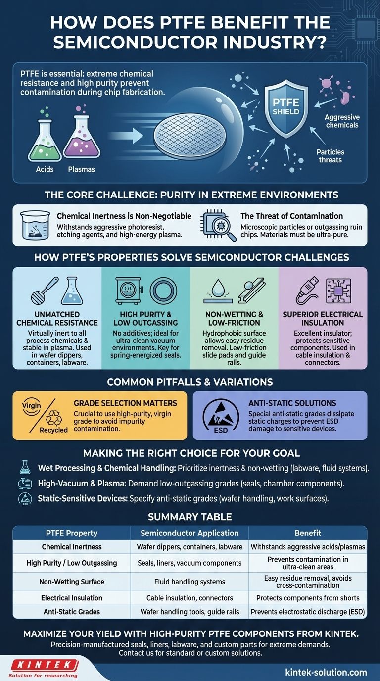
In short, PTFE is essential to the semiconductor industry because its extreme chemical resistance and high purity prevent contamination during chip fabrication. It provides a stable, non-reactive material that can withstand the aggressive chemicals, plasmas, and cleanroom conditions required to produce modern microelectronics safely and efficiently.
The core challenge in semiconductor manufacturing is a constant battle against contamination in highly corrosive environments. PTFE is a critical material in this fight because it offers a unique combination of chemical inertness, high purity, and physical stability that other materials cannot match.
The Core Challenge: Purity in Extreme Environments
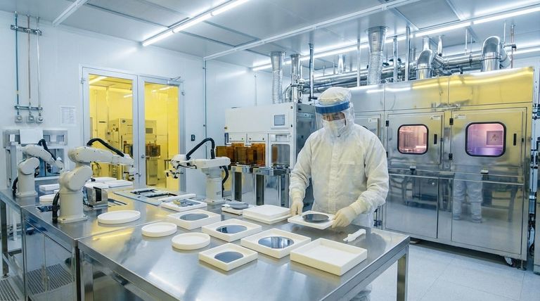
To understand PTFE's role, we must first appreciate the hostile environment of a semiconductor fabrication plant, or "fab." Manufacturing a silicon wafer into finished chips involves hundreds of steps, many of which are incredibly sensitive.
Why Chemical Inertness is Non-Negotiable
The production process relies on extremely aggressive substances. Strong acids are used in the photoresist and etching stages, and high-energy plasma is used to deposit or remove materials at the atomic level.
Any material used for tools, containers, or seals in these processes must not react with or degrade from contact with these chemicals.
The Threat of Contamination
The microscopic scale of modern transistors means that even a minuscule amount of foreign material can ruin a chip. This contamination can come from a tool that leaches chemicals or a surface that sheds particles.
Therefore, all materials in the process path must be exceptionally pure and stable, contributing nothing to the environment. This includes having low outgassing characteristics, meaning they don't release trapped gases when placed in a vacuum.
How PTFE's Properties Solve Semiconductor Challenges
PTFE's distinct molecular structure gives it a set of properties that directly addresses the industry's primary challenges. It acts as a shield, protecting the delicate manufacturing process from disruption.
Unmatched Chemical Resistance
PTFE is virtually inert to the entire range of aggressive chemicals used in chip manufacturing. It is used for wafer dippers, containers, fasteners, and custom labware precisely because it will not break down when exposed to strong acids.
Crucially, it also remains chemically stable when exposed to plasma, making it suitable for components inside etching and deposition chambers.
High Purity and Low Outgassing
High-purity grades of PTFE do not contain additives or fillers that could leach out and contaminate a wafer. Its stable nature means it's ideal for use in ultra-clean vacuum environments.
This is why PTFE is a primary material for spring-energized seals in wafer handling systems and process tools, ensuring a clean, leak-free vacuum.
Non-Wetting and Low-Friction Surfaces
PTFE's surface is non-wetting (hydrophobic), which allows chemical residues to be removed easily and completely. This prevents cross-contamination between process steps and ensures product purity.
Its low-friction properties also make it ideal for mechanical parts like guide rails and low-friction slide pads where smooth, clean movement is required without lubricants.
Superior Electrical Insulation
PTFE is an excellent electrical insulator. This property is leveraged in applications like cable insulation and connectors for circuit boards, where it protects sensitive electronic components from short circuits and environmental factors.
Common Pitfalls and Variations
While PTFE is highly effective, not all PTFE is created equal. Selecting the wrong type can undermine its benefits.
The Importance of Grade Selection
For semiconductor applications, it is critical to use a high-purity, virgin grade of PTFE. Recycled or lower-quality grades may contain impurities that can cause contamination, defeating the primary purpose of using the material.
The Anti-Static Solution
Standard PTFE is an excellent insulator, but this means it can build up a static charge. In environments with static-sensitive devices, this can lead to electrostatic discharge (ESD) events that destroy components.
To solve this, specialized anti-static grades of PTFE are available. These grades are engineered to safely dissipate static charges, making them the superior choice for static-sensitive manufacturing areas.
Making the Right Choice for Your Goal
Selecting the correct form and grade of PTFE is dependent on the specific manufacturing step and environment.
- If your primary focus is wet processing and chemical handling: Prioritize PTFE's chemical inertness and non-wetting properties for custom labware, containers, and fluid systems.
- If your primary focus is high-vacuum or plasma environments: Demand PTFE grades with certified low-outgassing characteristics for seals, liners, and chamber components.
- If your primary focus is managing static-sensitive devices: Specify anti-static grade PTFE for wafer handling tools, guide rails, and work surfaces to prevent ESD damage.
Ultimately, leveraging PTFE's unique properties is a foundational strategy for ensuring reliability and yield in modern semiconductor fabrication.
Summary Table:
| PTFE Property | Semiconductor Application | Benefit |
|---|---|---|
| Chemical Inertness | Wafer dippers, containers, labware | Withstands aggressive acids and plasmas without degradation |
| High Purity / Low Outgassing | Seals, liners, vacuum chamber components | Prevents contamination in ultra-clean environments |
| Non-Wetting Surface | Fluid handling systems | Allows for easy, complete residue removal, preventing cross-contamination |
| Electrical Insulation | Cable insulation, connectors | Protects sensitive components from short circuits |
| Anti-Static Grades | Wafer handling tools, guide rails | Prevents electrostatic discharge (ESD) damage to static-sensitive devices |
Maximize your semiconductor manufacturing yield with high-purity PTFE components from KINTEK.
Our precision-manufactured PTFE seals, liners, labware, and custom parts are engineered to meet the extreme demands of the semiconductor industry. We provide the material purity and performance you need to protect your processes from contamination in corrosive and high-vacuum environments.
Whether you require standard components or custom fabrication from prototypes to high-volume orders, KINTEK delivers the reliability your production depends on.
Contact our experts today to discuss your specific application requirements and ensure your process integrity.
Visual Guide
Related Products
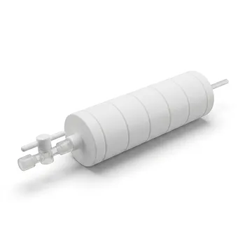
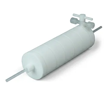
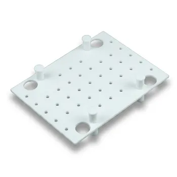
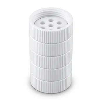
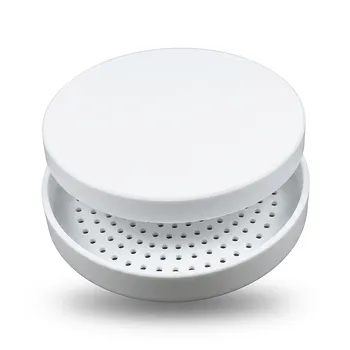
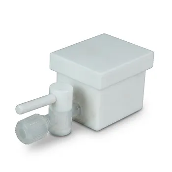
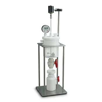
- Custom PTFE Filtration System Acid Resistant High Purity Semiconductor Grade Chemical Processing Filter
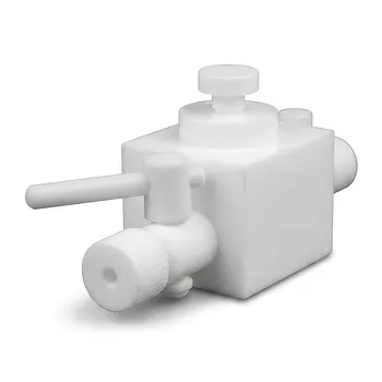
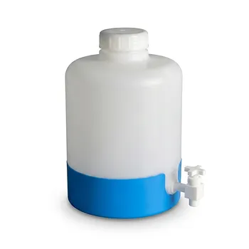
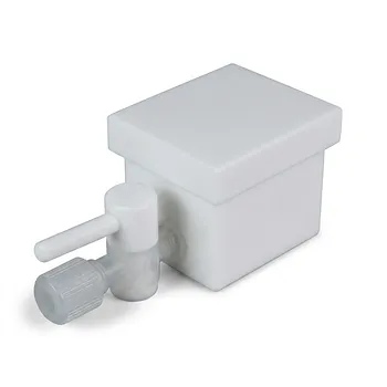
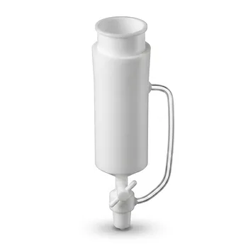
- High Corrosion Resistant PTFE Faucet Polytetrafluoroethylene Valve for Chemical Storage Drums and Fluid Transfer Systems Customizable Industrial Grade
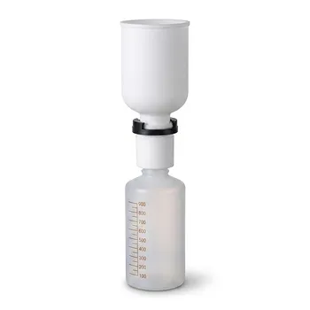
- PTFE PFA Vacuum Filtration System Corrosion Resistant Customizable Shatterproof Laboratory Device
- PTFE Corrosion Resistant Filter with PFA Valve Connections and Integrated Sieve Plate
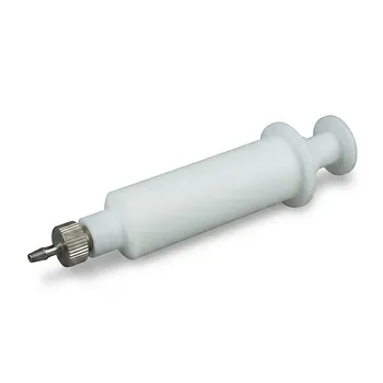
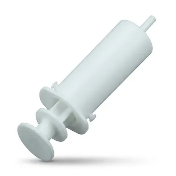
- High Temperature Chemical Resistant 50ml PTFE Syringe Customized Teflon Injector with Threaded Seal for Trace Analysis
People Also Ask
- What sizes and pore options are available for PTFE filters? Choose the Right Filter for Your Application
- Why are PTFE filters advantageous for gravimetric analysis? Achieve Unmatched Accuracy and Precision
- What temperature resistance do PTFE filters offer? Unmatched Thermal Stability from -200°C to +260°C
- Which chemicals are fully compatible with PTFE filters? Discover Unmatched Chemical Resistance
- How does the hydrophobicity of PTFE filters benefit their use? Ensure Uninterrupted Gas Flow and Solvent Filtration