Glass weave style directly impacts phase response by introducing variations in the substrate's effective dielectric constant (Dk). A more open glass weave creates larger areas of pure resin next to bundles of glass fiber. This non-uniformity causes the signal's propagation speed to vary as it travels along a trace, leading to unpredictable phase shifts, a phenomenon known as the fiber weave effect.
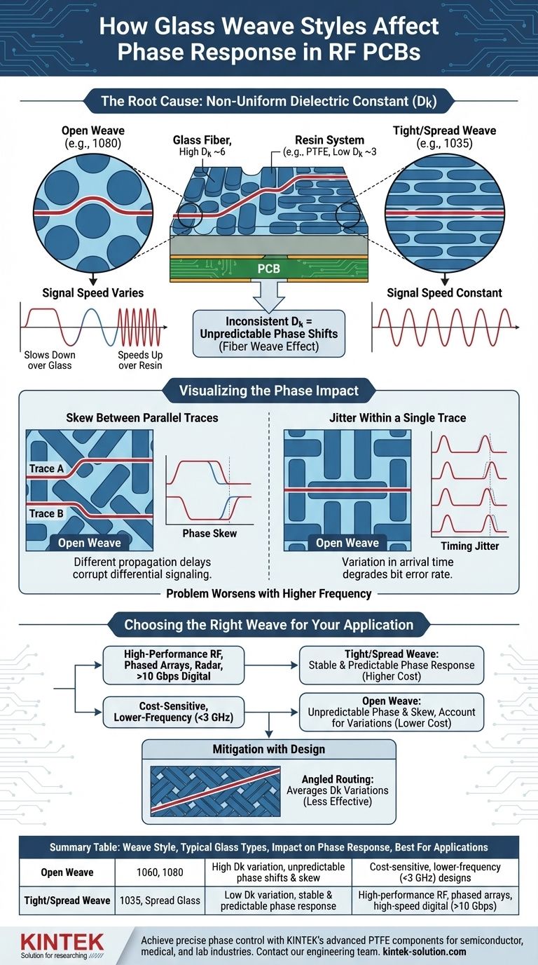
The central issue is dielectric inconsistency. A PCB substrate is a composite of glass (high Dk) and resin (low Dk). An open weave creates a non-uniform Dk landscape, causing a signal's phase to shift unpredictably depending on whether its trace runs over glass or resin.
The Root Cause: The Fiber Weave Effect
To understand the impact on phase, you must first understand the material itself. RF circuit boards are not monolithic; they are a composite material.
A Composite of Two Materials
A standard PCB substrate is made of woven glass fabric that is impregnated with a resin system (like epoxy, PTFE, or other polymers). These two components have very different electrical properties.
- Glass Fiber: Has a relatively high dielectric constant, typically around Dk 6.
- Resin System: Has a much lower dielectric constant, often around Dk 3.
The "effective Dk" of the final laminate is an average of these two values, but this is only true on a macroscopic scale.
How Weave Style Creates Inconsistency
The way the glass is woven determines how uniform the Dk is on a microscopic level, which is what a high-frequency signal actually experiences.
- An open weave (like 106 or 1080 glass) is like a wide net with large holes. This creates significant resin-rich pockets between the glass bundles.
- A tight or spread weave (like 1035 or mechanically spread glass) is like a fine, tightly woven fabric. The glass and resin are distributed much more evenly.
A signal trace running on a board with an open weave can alternate between traveling over a high-Dk glass bundle and a low-Dk resin pocket.
The Impact on Signal Propagation
The propagation speed of an electrical signal is inversely proportional to the square root of the dielectric constant.
- Higher Dk (over glass): The signal slows down.
- Lower Dk (over resin): The signal speeds up.
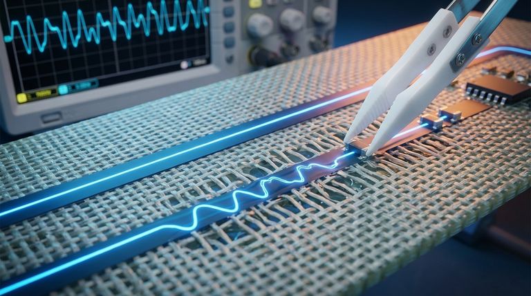
This constant speeding up and slowing down along the trace path directly translates into unpredictable variations in the signal's phase upon arrival. This is the fiber weave effect.
Visualizing the Phase Impact
The fiber weave effect manifests in two primary ways that are detrimental to high-performance systems.
Skew Between Parallel Traces
Consider two perfectly matched traces running in parallel, as in a differential pair. If one trace happens to run primarily over a glass bundle and the adjacent trace runs over a resin-rich area, they will have different propagation delays. This introduces phase skew, corrupting differential signaling.
Jitter Within a Single Trace
Even a single trace will experience this effect. As the signal path crosses over glass bundles and resin pockets, its arrival time will vary slightly. This variation from the ideal timing is known as timing jitter, which can degrade the bit error rate in high-speed digital systems.
Why It Worsens with Frequency
This effect becomes significantly more problematic as frequencies increase. At higher frequencies, the signal's wavelength becomes shorter and can be comparable in size to the openings in the glass weave. This makes the signal highly sensitive to the small, localized Dk variations.
Understanding the Trade-offs
Choosing a substrate is not just about picking the best electrical performance; it involves balancing practical constraints.
Performance vs. Cost
Substrates with tight, flat, or spread glass weaves offer superior phase stability and are the clear choice for demanding applications. However, these advanced materials are significantly more expensive than standard laminates using common open weaves.
Mitigating with Design
If a tighter weave is not an option due to cost, some designers route critical traces at a slight angle (e.g., 10 degrees) relative to the weave's axis. This ensures the trace path averages out the Dk variations by crossing over glass and resin more evenly, though it is a less effective solution than using a better material.
When Is It a Problem?
For many lower-frequency RF circuits (e.g., below 3 GHz) or digital designs that are not pushing speed limits, the fiber weave effect may be negligible. The key is to evaluate the phase and timing budget of your specific application.
Choosing the Right Weave for Your Application
Your choice of material should be a deliberate decision based on the specific performance requirements of your design.
- If your primary focus is high-performance phased arrays, radar, or satellite communications: You must select a substrate with a flat or spread glass weave to ensure predictable phase coherence.
- If your primary focus is high-speed digital interfaces (>10 Gbps): Use a tighter weave material to minimize differential pair skew and reduce data-dependent jitter.
- If your primary focus is cost-sensitive or lower-frequency applications: A standard, more open weave may be sufficient, but you must account for potential performance variations in your design margins.
Ultimately, selecting the correct glass weave is a fundamental design choice that moves phase performance from an unpredictable variable to a reliable constant.
Summary Table:
| Weave Style | Typical Glass Types | Impact on Phase Response | Best For Applications |
|---|---|---|---|
| Open Weave | 1060, 1080 | High Dk variation, unpredictable phase shifts & skew | Cost-sensitive, lower-frequency (<3 GHz) designs |
| Tight/Spread Weave | 1035, Spread Glass | Low Dk variation, stable & predictable phase response | High-performance RF, phased arrays, high-speed digital (>10 Gbps) |
Achieve precise phase control in your RF PCBs with KINTEK's advanced PTFE components.
For semiconductor, medical, and laboratory industries requiring ultimate signal integrity, the substrate's dielectric properties are paramount. KINTEK specializes in manufacturing high-precision PTFE components—including custom seals, liners, and labware—that complement advanced PCB substrates by providing stable, low-loss performance.
Whether you need prototypes or high-volume production, our expertise in custom fabrication ensures your high-frequency designs meet stringent phase and timing requirements.
Contact our engineering team today to discuss how our components can enhance your next RF or high-speed digital project.
Visual Guide
Related Products
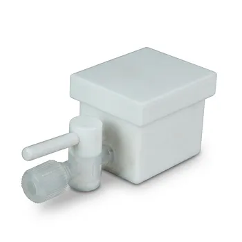
- Custom PTFE Corrosion Resistant Insulating Electrophoresis Reaction Cell with Septum and Valves for Low Background Trace Analysis
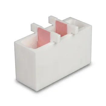
- Square PTFE Electrochemical Cell for Silicon Wafer Processing and Hydrofluoric Acid Resistance in Semiconductor and New Energy Research
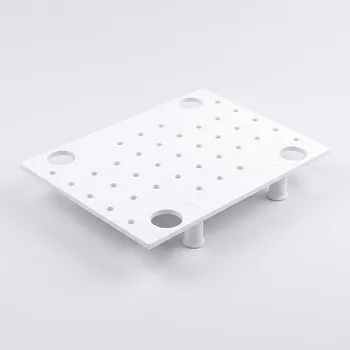
- High Temperature Resistant PTFE Thermal Insulation Board Corrosion Resistant Metal Free Fluoropolymer Stand for Ultra Clean Laboratories
People Also Ask
- What industries benefit most from custom PTFE parts? Solve Extreme Environment Challenges
- What are the key properties of PTFE valves? Ensure Purity, Safety, and Reliability in Demanding Processes
- How do PTFE valves and components support high-purity liquid transfer? Ensure Product Integrity with Inert Materials
- What specific advantages do PTFE valves offer? Unmatched Corrosion Resistance for Industrial Chemical Handling
- What are the key properties of Teflon (PTFE) used in custom parts? | Achieve Peak Performance