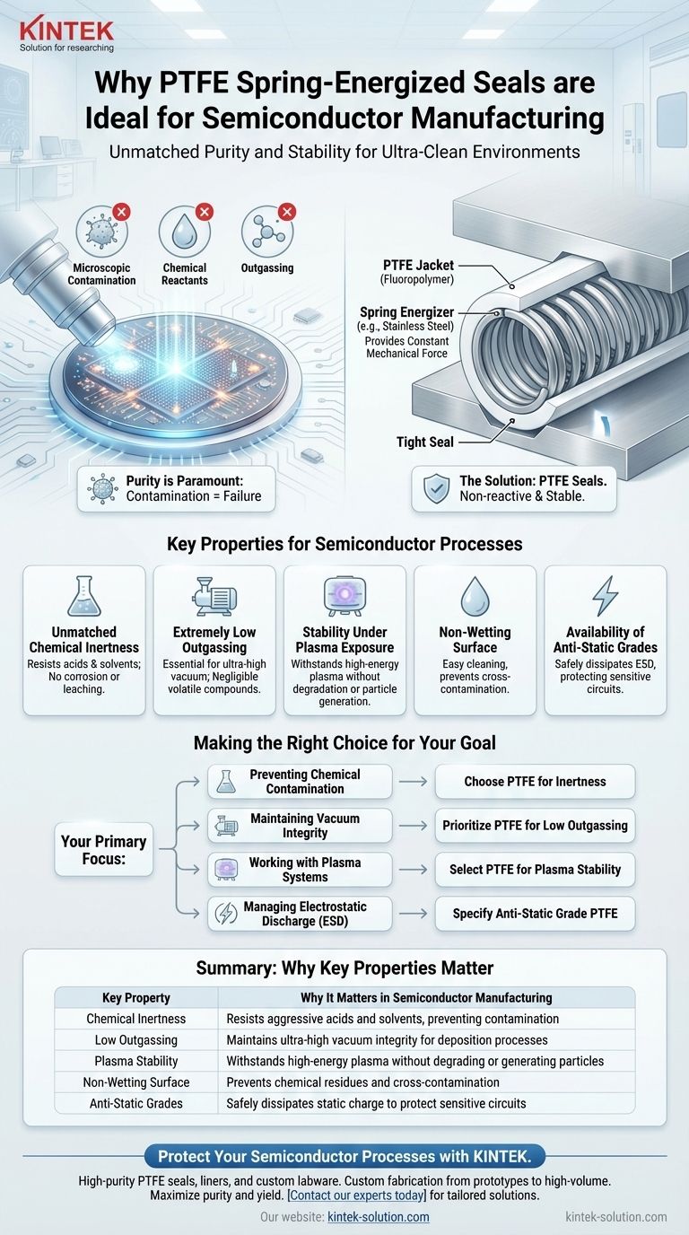
To be precise, PTFE spring-energized seals are ideal for semiconductor manufacturing because they possess an unmatched combination of chemical inertness, low outgassing characteristics, and stability in plasma environments. In an industry where microscopic contamination can destroy millions of dollars in product, these properties ensure the seal itself does not become a source of failure, protecting the ultra-clean conditions required for wafer fabrication.
The core challenge in semiconductor manufacturing is not simply sealing a system, but doing so without introducing any foreign material—be it a particle, a gas molecule, or a chemical reactant. PTFE spring-energized seals are the solution because they are fundamentally non-reactive and stable, safeguarding the purity of the process environment.
Why Purity is the Paramount Concern
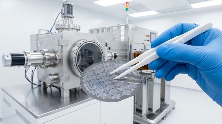
To understand the value of PTFE, you must first understand the extreme sensitivity of semiconductor fabrication. The goal is to create microscopic circuits on silicon wafers, and any deviation from a perfectly controlled environment can lead to defects.
The Microscopic Scale of Failure
The features on a modern microchip are measured in nanometers. A single, microscopic particle released from a degrading seal can land on a wafer and block a critical pathway, rendering the entire chip useless. This makes material stability non-negotiable.
The Hostile Chemical and Plasma Environment
Chip manufacturing relies on highly aggressive processes. This includes using strong acids for photoresist processes and employing high-energy plasma for etching away material. A seal must withstand this constant chemical and physical assault without breaking down.
The Need for Absolute Vacuum Integrity
Many key processes, such as deposition, occur in an ultra-high vacuum. A seal material that releases trapped gas—a phenomenon called outgassing—can alter the vacuum pressure and deposit unwanted molecules onto the wafer surface, compromising the integrity of the thin films being created.
Key Properties of PTFE Seals for Semiconductor Processes
PTFE's material science directly addresses the challenges of the semiconductor environment. The spring energizer simply provides the constant mechanical force needed for a tight seal, while the PTFE jacket provides the critical performance characteristics.
Unmatched Chemical Inertness
PTFE is resistant to nearly all industrial chemicals, including the strong acids and solvents used in semiconductor fabrication. This inertness ensures the seal will not corrode, swell, or leach contaminants into the process stream.
Extremely Low Outgassing
Compared to most elastomers, PTFE has exceptionally low outgassing properties. This makes it a superior choice for vacuum chambers, as it releases a negligible amount of volatile compounds that could otherwise contaminate the wafer.
Stability Under Plasma Exposure
Plasma etching and deposition are fundamental to chipmaking. PTFE remains chemically stable when exposed to these high-energy plasma environments, preventing it from degrading and generating particles that would cause defects.
Non-Wetting Surface
PTFE's non-wetting and non-stick characteristics are crucial for cleanliness. Chemical residues can be removed easily and completely, ensuring that no cross-contamination occurs between different process steps.
Availability of Anti-Static Grades
Electrostatic discharge (ESD) can instantly destroy the sensitive circuits on a wafer. PTFE is available in anti-static grades that safely dissipate static charge, making it an excellent choice for wafer handling and other static-sensitive applications.
Understanding the Trade-offs and Context
While ideal, it's important to view PTFE as a component within a larger system of material choices, each serving a specific purpose in maintaining purity.
The Role of the Spring Energizer
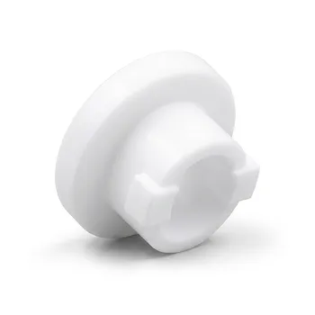
It is critical to remember that PTFE itself has poor elastic memory. The internal spring (typically made from stainless steel or other resilient alloys) provides the constant outward force required to maintain a seal against the mating surfaces. The design combines the spring's mechanical properties with the PTFE's chemical properties.
Beyond Sealing Applications
The same properties that make PTFE ideal for seals also make it a preferred material for other components in the fabrication plant. It is frequently used for custom labware, wafer dippers and containers, guide rails, and insulation, all in service of the same goal: preventing contamination.
Not All PTFE is Created Equal
The PTFE used in semiconductor applications is of a much higher purity and grade than that used for general industrial purposes. Sourcing from reputable suppliers who can certify the material's purity and trace-ability is essential to achieving the desired performance.
Making the Right Choice for Your Goal
Your specific application will determine which property of PTFE is most critical.
- If your primary focus is preventing chemical contamination: Choose PTFE for its unrivaled inertness, ensuring it will not react with aggressive acids, solvents, or precursors.
- If your primary focus is maintaining vacuum integrity: Prioritize PTFE for its low outgassing characteristics, which protect sensitive deposition and etch processes from molecular contamination.
- If your primary focus is working with plasma systems: Select PTFE for its proven stability under plasma exposure, avoiding seal degradation and subsequent particle generation.
- If your primary focus is managing electrostatic discharge (ESD): Specify an anti-static grade of PTFE to protect sensitive components from catastrophic damage during handling and processing.
Ultimately, choosing PTFE spring-energized seals is a strategic decision to safeguard process integrity and maximize yield in an environment where purity defines success.
Summary Table:
| Key Property | Why It Matters in Semiconductor Manufacturing |
|---|---|
| Chemical Inertness | Resists aggressive acids and solvents, preventing contamination |
| Low Outgassing | Maintains ultra-high vacuum integrity for deposition processes |
| Plasma Stability | Withstands high-energy plasma without degrading or generating particles |
| Non-Wetting Surface | Prevents chemical residues and cross-contamination |
| Anti-Static Grades | Safely dissipates static charge to protect sensitive circuits |
Protect your semiconductor processes with precision-engineered PTFE components from KINTEK.
Our high-purity PTFE seals, liners, and custom labware are designed to meet the extreme demands of semiconductor, medical, and laboratory environments. We specialize in custom fabrication from prototypes to high-volume orders, ensuring your systems achieve maximum purity and yield.
Contact our experts today to discuss your specific application and receive a solution tailored to your needs.
Visual Guide
Related Products
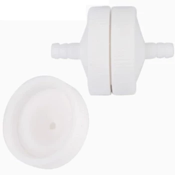
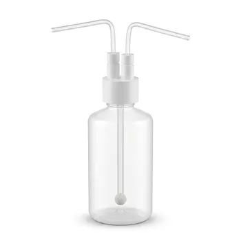
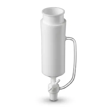
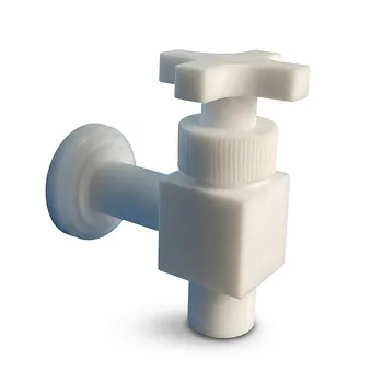
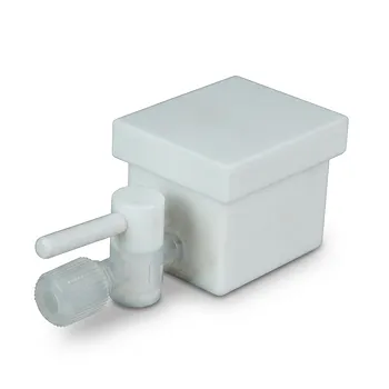
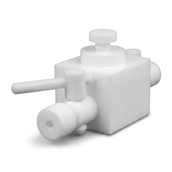
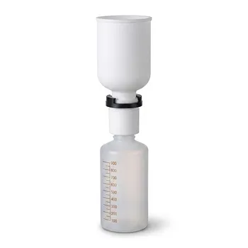
- Customizable PTFE Seals Filter Holders for Versatile Applications
- Customizable High Temperature Resistant Anti Static PTFE Insulating Gaskets Flame Retardant Corrosion Proof Industrial Seals
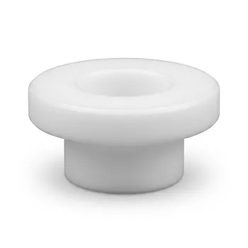
- Custom PTFE Insulating Gaskets and Corrosion Resistant Fluoropolymer Seals for Industrial Electrical Applications
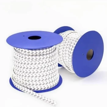
- Custom PTFE Sealing Tapes for Industrial and High Tech Applications
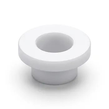
- Custom PTFE Insulating Gaskets Corrosion Resistant Teflon Seals Tailored Engineering Plastic Components
People Also Ask
- What aerospace applications utilize PTFE seals? Ensure Reliability in Extreme Conditions
- What are the benefits of using PTFE seals in demanding industries? Solve Extreme Sealing Challenges
- What is the typical temperature range for PTFE seals? -200°C to 260°C Performance
- How are custom PTFE parts used in the automotive sector? Enhance Vehicle Performance & Durability
- What are the drawbacks of PTFE seals? Key Limitations and Design Considerations