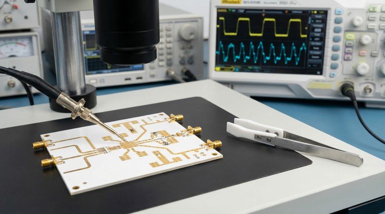
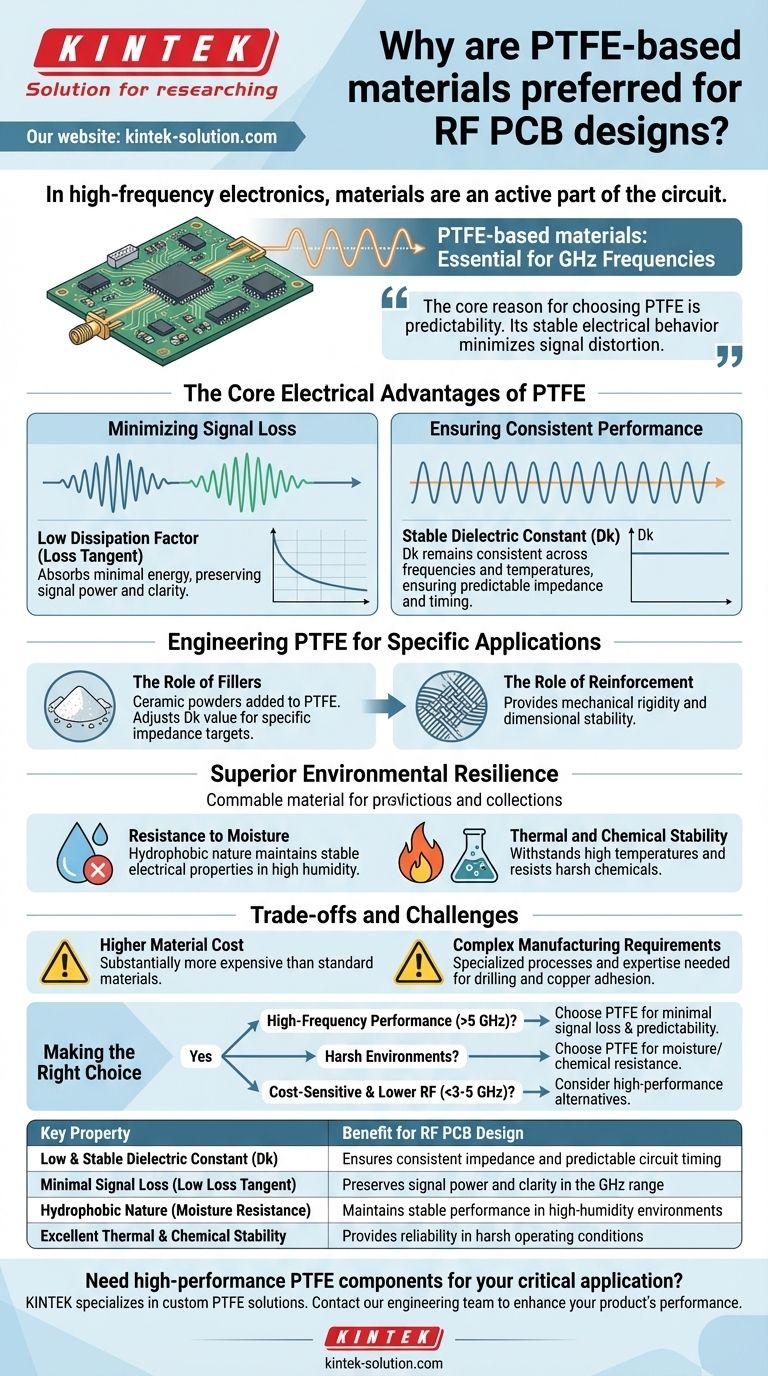
In high-frequency electronics, materials are not just structural—they are an active part of the circuit. PTFE-based materials are preferred for Radio Frequency (RF) PCB designs because their core electrical properties, primarily a very low and stable dielectric constant (Dk) and minimal signal loss (low loss tangent), are essential for maintaining signal integrity as frequencies climb into the gigahertz range.
The core reason for choosing PTFE is predictability. In RF design, the PCB material itself can distort the signal, but PTFE's stable electrical behavior across a wide range of frequencies and temperatures minimizes this distortion, ensuring the final circuit performs exactly as it was simulated.
The Core Electrical Advantages of PTFE
The choice of a PCB laminate in RF engineering is driven by its impact on the electromagnetic waves traveling through the circuit. PTFE's unique molecular structure gives it two critical advantages.
Minimizing Signal Loss (Low Dissipation Factor)
At high frequencies, the insulating material of a PCB can absorb energy from the electrical signal, converting it into wasted heat. This phenomenon is known as dielectric loss.
PTFE has an exceptionally low dissipation factor (also called loss tangent). This means it absorbs very little energy, allowing the RF signal to travel through the circuit with minimal attenuation, preserving its power and clarity.
Ensuring Consistent Performance (Stable Dielectric Constant)
The dielectric constant (Dk) of a material dictates how fast a signal travels and influences the physical dimensions of critical circuit elements like filters and antennas.
While PTFE has a low Dk, its most important characteristic is stability. Its Dk remains remarkably consistent across a vast range of frequencies and operating temperatures. This stability ensures that the circuit's impedance and timing remain predictable, which is non-negotiable for reliable RF performance.
Engineering PTFE for Specific Applications
Pure PTFE is a soft material. To be useful in a rigid PCB, it is combined with other materials to create a composite laminate with tailored properties.
The Role of Fillers
Manufacturers add ceramic powders and other fillers to the PTFE matrix. These fillers are used to precisely engineer the material's final Dk value.
This allows designers to select from a wide range of laminates with different Dk values to meet specific impedance or performance targets, while still retaining the low-loss benefits of PTFE.
The Role of Reinforcement
To provide mechanical rigidity and improve dimensional stability, PTFE is often reinforced, typically with woven glass or other structural materials.
This reinforcement gives the laminate the strength to withstand the manufacturing process and the stresses of its final operating environment without warping or damage.
Superior Environmental Resilience
RF circuits often operate in demanding conditions where environmental factors can degrade performance. PTFE's inherent properties provide a robust defense against these challenges.
Resistance to Moisture
Moisture absorption can dramatically alter a material's Dk, leading to unpredictable circuit behavior. PTFE is hydrophobic, meaning it repels water.
This resistance ensures the board's electrical properties remain stable even in high-humidity environments, a critical factor for outdoor, automotive, or aerospace applications.
Thermal and Chemical Stability
PTFE is one of the most chemically inert and thermally stable polymers available. It can withstand very high temperatures and is resistant to nearly all industrial chemicals and solvents.
This makes it an ideal choice for electronics deployed in harsh industrial settings where exposure to extreme conditions is common.
Understanding the Trade-offs and Challenges
Despite its exceptional performance, PTFE is not the default choice for every design. Its advantages come with significant trade-offs that must be considered.
Higher Material Cost
PTFE-based laminates are substantially more expensive than standard materials like FR-4. Their use is typically justified only when the performance requirements demand it.
Complex Manufacturing Requirements
PTFE's unique properties make it challenging to process. Its softness can lead to smearing during drilling, and its non-stick nature requires special chemical or plasma treatments to ensure copper layers adhere properly.
These specialized processes increase fabrication costs and require a manufacturer with specific expertise in handling RF materials.
Making the Right Choice for Your Application
Selecting the right PCB material is a balance of performance, cost, and manufacturability. The decision to use PTFE should be driven by the specific demands of your design.
- If your primary focus is high-frequency performance (above 5 GHz): PTFE is often the necessary choice to manage signal loss and ensure predictable circuit behavior.
- If your design must operate in harsh environments: PTFE's inherent resistance to moisture, chemicals, and high temperatures makes it a highly reliable option.
- If your design is cost-sensitive and operates at lower RF frequencies (below 3-5 GHz): High-performance alternatives to PTFE may offer an acceptable balance of cost and performance.
Ultimately, selecting a PTFE-based material is an engineering decision to prioritize predictable electrical performance and environmental reliability above all else.
Summary Table:
| Key Property | Benefit for RF PCB Design |
|---|---|
| Low & Stable Dielectric Constant (Dk) | Ensures consistent impedance and predictable circuit timing |
| Minimal Signal Loss (Low Loss Tangent) | Preserves signal power and clarity in the GHz range |
| Hydrophobic Nature (Moisture Resistance) | Maintains stable performance in high-humidity environments |
| Excellent Thermal & Chemical Stability | Provides reliability in harsh operating conditions |
Need high-performance PTFE components for your critical application?
KINTEK specializes in the precision manufacturing of custom PTFE seals, liners, labware, and complex components. Our expertise is critical for industries where material performance is non-negotiable, including semiconductor, medical, laboratory, and specialized industrial applications.
We partner with you from prototype through high-volume production to ensure your designs achieve maximum reliability and signal integrity. Contact our engineering team today to discuss your project requirements and how our custom PTFE solutions can enhance your product's performance.
Visual Guide
Related Products
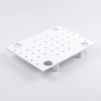
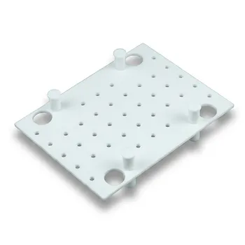
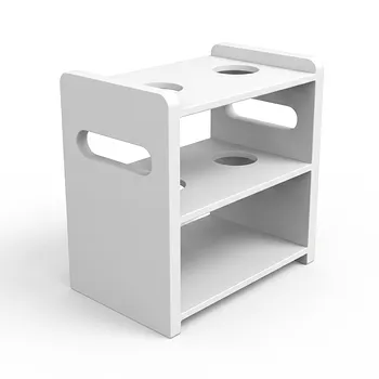
- High Temperature Resistant PTFE Thermal Insulation Board Corrosion Resistant Metal Free Fluoropolymer Stand for Ultra Clean Laboratories
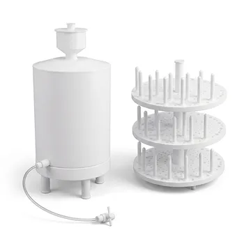
- Customizable PTFE Heat Insulation Plate High Temperature Corrosion Resistant Laboratory Support Layered Multi Tier Stand
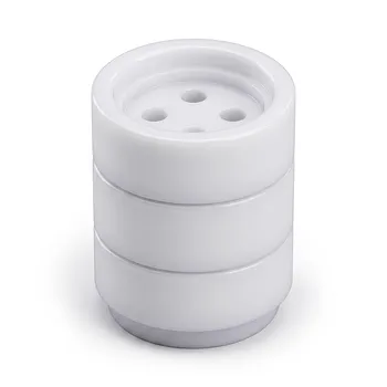
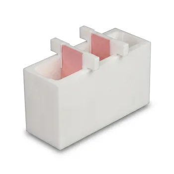
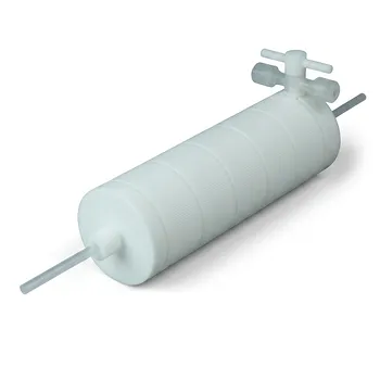
- Custom PTFE Multi Layer Filtration Plates Corrosion Resistant Low Background Lab Grade Filter Assemblies
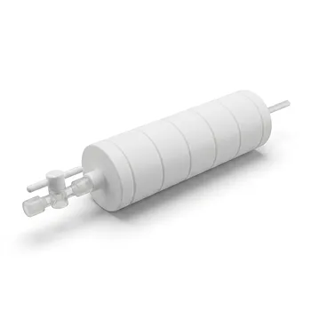
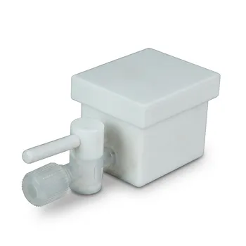
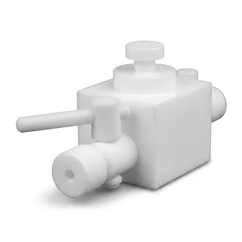
- PTFE Corrosion Resistant Filter with PFA Valve Connections and Integrated Sieve Plate
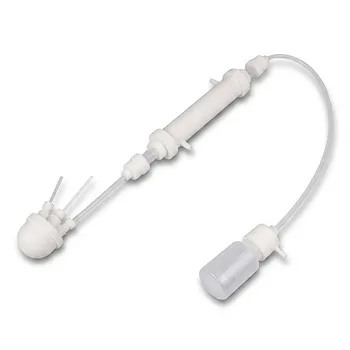
- Custom PTFE Condensation Reflux Apparatus with Serpentine Coil and Flask Collection System for Corrosive Chemical Processing
People Also Ask
- Can you provide examples of industries where PTFE bars have been successfully applied? Discover Key Applications
- What are the limitations of pure PTFE in high temperature applications? Understanding the 200°C Ceiling
- What factors should be considered when choosing PTFE bars for chemical applications? Select the Right Grade for Your Process
- What advantages do PTFE bars offer in chemical industries? Ensure Safety and Efficiency in Demanding Applications
- What are some future trends in the application of PTFE bars in the chemical industry? Engineering for Extreme Performance