Manufacturing a PTFE PCB requires highly specialized processes that differ significantly from standard circuit board fabrication. These steps include plasma treatment to activate the material's inert surface for copper adhesion, precision laser drilling to avoid damaging the soft substrate, and carefully controlled high-temperature lamination to bond layers without causing deformation.
The core challenge of working with PTFE is its combination of exceptional electrical properties and difficult physical characteristics. While its low dielectric constant is ideal for high-frequency signals, its chemical inertness and softness demand a complete re-thinking of standard manufacturing techniques to ensure reliability.
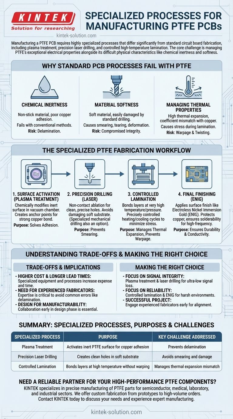
Why Standard PCB Processes Fail with PTFE
Before detailing the specialized workflow, it's essential to understand why conventional methods used for materials like FR-4 are inadequate for Polytetrafluoroethylene (PTFE). The material's inherent properties present unique obstacles at every stage.
The Challenge of Chemical Inertness
PTFE is, by design, a non-stick material. This inertness makes it nearly impossible for copper foil to form a strong, reliable bond with the substrate using conventional adhesion methods.
Without proper surface treatment, copper layers will peel away, a catastrophic failure known as delamination.
The Problem of Material Softness
PTFE is a soft material, which poses a significant problem for mechanical fabrication. Standard drilling can easily cause smearing, tearing, or deformation around the hole.
This damage compromises the integrity of plated through-holes, which are critical for connecting different layers of the circuit. Minimal clamping pressure must also be used to avoid distorting the entire board.
Managing Thermal Properties
While PTFE is stable at high temperatures, it has a higher coefficient of thermal expansion than copper. During the high-temperature lamination process, this mismatch can introduce significant stress.
Uncontrolled heating and cooling cycles will cause the board to warp or twist, destroying its dimensional stability and rendering the circuit useless.
The Specialized PTFE Fabrication Workflow
To overcome these challenges, manufacturers employ a sequence of highly controlled and specialized processes. Each step is tailored specifically to the unique properties of PTFE.
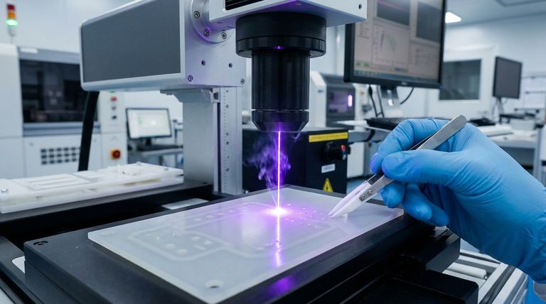
Step 1: Surface Activation via Plasma Treatment
To solve the adhesion problem, the PTFE surface must be chemically modified. This is most commonly done using plasma treatment.
The board is placed in a vacuum chamber where gas is excited into a plasma state. This plasma microscopically etches the PTFE surface, creating anchor points that allow the copper to form a strong mechanical bond.
Step 2: Precision Drilling and Machining
To create clean, precise holes without damaging the soft material, fabricators turn to advanced techniques. Laser drilling is often the preferred method as it's a non-contact process that ablates material cleanly.
When mechanical drilling is used, it requires specialized micro-drill bits, slower cutting speeds, and higher feed rates to minimize heat buildup and prevent material from smearing.
Step 3: Controlled High-Temperature Lamination
Bonding multiple layers of PTFE and copper requires a lamination process that takes place at very high temperatures and pressures.
This is done in specialized presses with precisely controlled heating and cooling cycles. The goal is to allow the materials to bond securely while minimizing the internal stress caused by thermal expansion, thus preventing warpage.
Step 4: Final Finishing
Once the core fabrication is complete, a surface finish is applied to protect the exposed copper and ensure solderability.
ENIG (Electroless Nickel Immersion Gold) is a very common choice for PTFE PCBs. It provides a flat, durable, and highly conductive surface well-suited for high-frequency applications and demanding environments.
Understanding the Trade-offs
Opting for a PTFE substrate has significant implications for any project. Understanding these trade-offs is critical for making an informed decision.
Higher Cost and Longer Lead Times
The specialized equipment, controlled processes, and expert handling required for PTFE fabrication make it significantly more expensive than working with standard materials like FR-4. The complexity also translates to longer manufacturing lead times.
The Need for Experienced Fabricators
Not all PCB manufacturers have the equipment or expertise to process PTFE correctly. The risk of fabrication errors like delamination, poor hole quality, or warpage is high with an inexperienced vendor. Partner selection is a critical factor for success.
Design for Manufacturability is Crucial
Designers cannot simply swap FR-4 for PTFE in a layout. They must account for the material's properties, such as its dimensional stability and softness. Collaborating with the fabricator early in the design phase is essential to avoid costly errors.
Making the Right Choice for Your Application
The decision to use PTFE should be driven by strict performance requirements. The specialized manufacturing process is a means to an end—unlocking the material's superior electrical capabilities.
- If your primary focus is signal integrity in RF/microwave circuits: The investment in plasma treatment and laser drilling is non-negotiable to achieve the ultra-low signal loss that PTFE promises.
- If your primary focus is reliability in harsh environments: Controlled lamination and a high-quality surface finish like ENIG are critical to prevent delamination and ensure long-term performance under thermal stress or chemical exposure.
- If your primary focus is a successful project outcome: You must engage with an experienced PTFE fabricator early to align your design with their specific manufacturing capabilities and constraints.
Ultimately, mastering PTFE manufacturing is about transforming a difficult material into a high-performance electronic asset.
Summary Table:
| Specialized Process | Purpose | Key Challenge Addressed |
|---|---|---|
| Plasma Treatment | Activates inert PTFE surface for copper adhesion | Prevents delamination |
| Precision Laser Drilling | Creates clean holes in soft substrate | Avoids smearing and damage |
| Controlled Lamination | Bonds layers at high temperature without warping | Manages thermal expansion mismatch |
Need a reliable partner for your high-performance PTFE components?
KINTEK specializes in the precise manufacturing of PTFE parts—from seals and liners to complex labware and custom components. Our expertise in handling challenging materials like PTFE ensures your projects for the semiconductor, medical, laboratory, and industrial sectors benefit from superior reliability and performance.
We offer custom fabrication from prototypes to high-volume orders, prioritizing the precision and care your application demands.
Contact KINTEK today to discuss your PTFE component needs and experience the difference expert manufacturing makes.
Visual Guide
Related Products
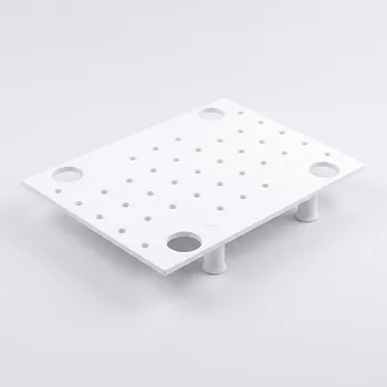
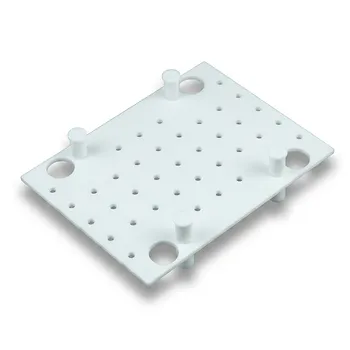
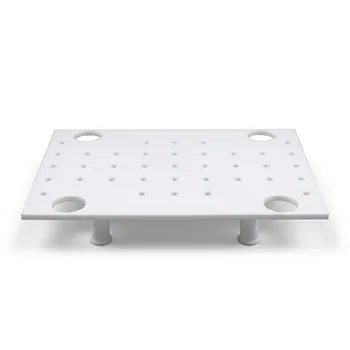
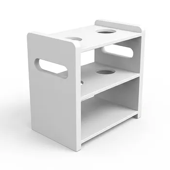
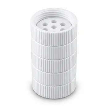
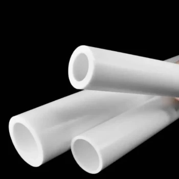
- High Temperature Resistant PTFE Thermal Insulation Board Corrosion Resistant Metal Free Fluoropolymer Stand for Ultra Clean Laboratories
- Customizable PTFE Heat Insulation Plate High Temperature Corrosion Resistant Laboratory Support Layered Multi Tier Stand
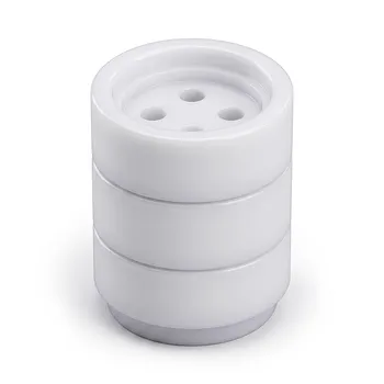
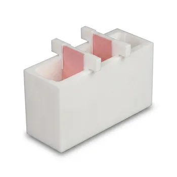
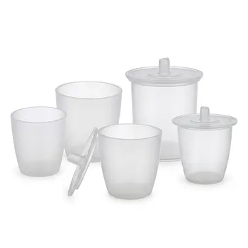
- Custom PTFE Multi Layer Filtration Plates Corrosion Resistant Low Background Lab Grade Filter Assemblies
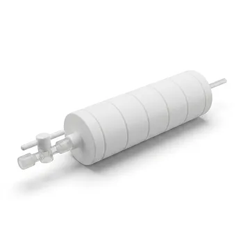
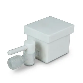
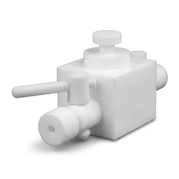
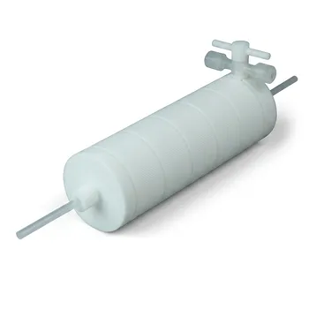
- PTFE Corrosion Resistant Filter with PFA Valve Connections and Integrated Sieve Plate
- PTFE Anti Scald Heat Insulation Sleeve Hot Plate Support Feet Laboratory Benchtop Protection Customizable Thermal Barrier
People Also Ask
- What are some future trends in the application of PTFE bars in the chemical industry? Engineering for Extreme Performance
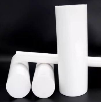
- What are the primary applications of PTFE bars in the chemical industry? Solve Your Toughest Corrosion Problems
- Can you provide examples of industries where PTFE bars have been successfully applied? Discover Key Applications
- How can the lifespan and performance of PTFE bars be maintained? A Guide to Proactive Care
- What advantages do PTFE bars offer in chemical industries? Ensure Safety and Efficiency in Demanding Applications