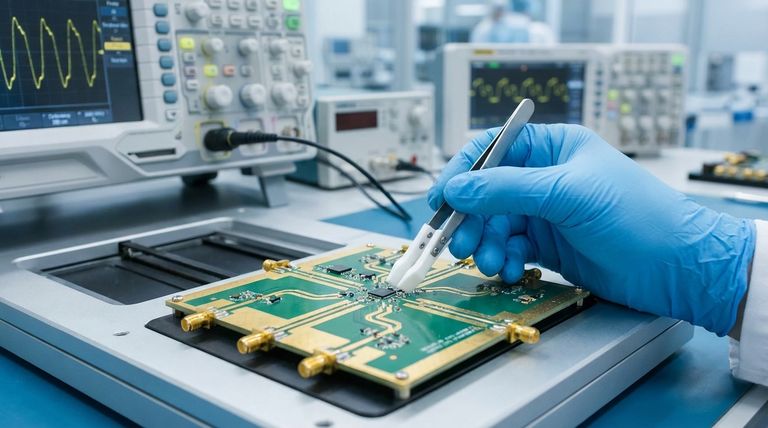
At its core, PTFE is a high-performance PCB material defined by its exceptional electrical properties at high frequencies and its remarkable resilience to heat and chemicals. This combination makes it the material of choice for the most demanding electronic applications, such as RF/microwave circuits, aerospace systems, and industrial sensors operating in harsh environments.
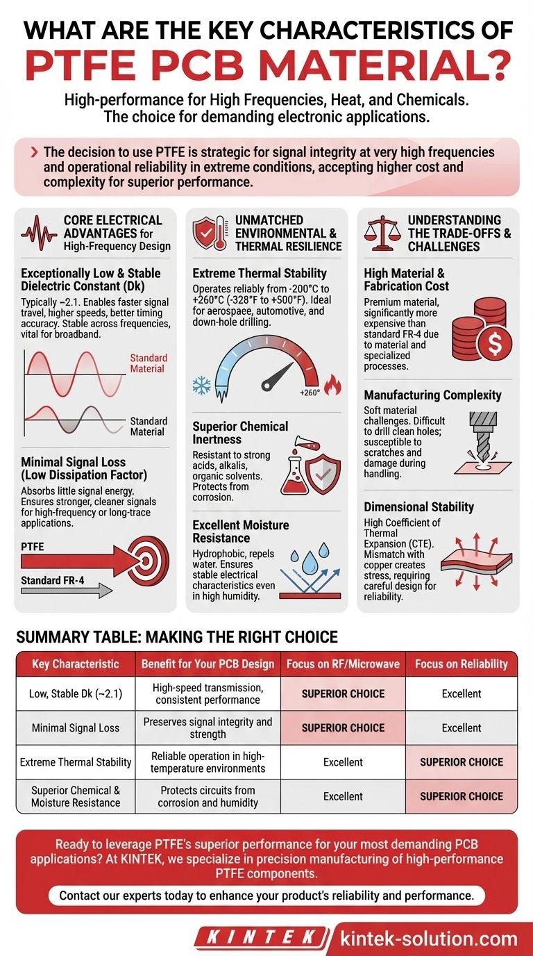
The decision to use PTFE is a strategic one. You choose it when signal integrity at very high frequencies and operational reliability in extreme conditions are non-negotiable, accepting the higher cost and manufacturing complexity as a necessary trade-off for its superior performance.
The Core Electrical Advantages for High-Frequency Design
The primary reason engineers specify PTFE is for its behavior with high-frequency signals. Unlike standard materials like FR-4, PTFE is engineered to preserve the integrity of signals that oscillate billions of times per second.
Exceptionally Low and Stable Dielectric Constant (Dk)
PTFE's dielectric constant is very low, typically around 2.1. A lower Dk allows electrical signals to travel faster through the circuit trace, enabling higher processing speeds and better timing accuracy.
Crucially, this Dk remains remarkably stable across a wide range of frequencies. This consistency is vital for broadband applications where the device must perform reliably from low to very high frequencies without signal distortion.
Minimal Signal Loss (Low Dissipation Factor)
PTFE has a very low dissipation factor (or loss tangent). This means it absorbs very little of a signal's energy as it passes through the material.
For high-frequency or long-trace applications, this low loss ensures a stronger, cleaner signal arrives at its destination, which is critical for sensitive receivers and high-power transmitters.
Unmatched Environmental and Thermal Resilience
Beyond its electrical performance, PTFE is known for its ability to withstand conditions that would cause other materials to fail.
Extreme Thermal Stability
PTFE PCBs can operate reliably across an exceptionally wide temperature range, often cited from -200°C to +260°C (-328°F to +500°F).
This makes it an ideal substrate for electronics deployed in aerospace, automotive, or down-hole drilling applications where extreme temperature swings are common.
Superior Chemical Inertness
PTFE is highly resistant to almost all common chemicals, including strong acids, alkalis, and organic solvents. This inertness protects the circuit from degradation in corrosive industrial or chemical processing environments.
Excellent Moisture Resistance
The material is hydrophobic, meaning it repels water and has extremely low moisture absorption. This property ensures its electrical characteristics, like Dk, remain stable even in high-humidity conditions, preventing performance drift over time.
Understanding the Trade-offs and Challenges
While its performance is outstanding, specifying PTFE is not without its challenges. Understanding these trade-offs is key to making an informed decision.
High Material and Fabrication Cost
PTFE is a premium material, and its PCBs are significantly more expensive than those made from standard FR-4. Both the raw laminate and the specialized manufacturing processes contribute to the higher cost.
Manufacturing Complexity
PTFE is a soft material, which presents unique challenges during fabrication. Drilling clean holes without smearing is difficult and requires specialized techniques. Its softness also makes it more susceptible to scratches and damage during handling.
Dimensional Stability
PTFE has a high coefficient of thermal expansion (CTE) compared to the copper used for traces and planes. This mismatch can create stress on plated through-holes and solder joints during thermal cycling, requiring careful design and manufacturing controls to ensure long-term reliability.
Making the Right Choice for Your Goal
Selecting a PCB material is about aligning its properties with your project's most critical requirements.
- If your primary focus is RF/Microwave Performance (above 3 GHz): PTFE is the superior choice for its low, stable Dk and minimal signal loss, which are essential for maintaining signal integrity.
- If your primary focus is Reliability in Harsh Environments: Specify PTFE when your device will be exposed to extreme temperatures, corrosive chemicals, or high humidity.
- If your primary focus is a Balance of Performance and Cost: Consider alternatives like Rogers 4000 series or other ceramic-filled hydrocarbon materials that offer good high-frequency performance with easier manufacturing and lower costs than pure PTFE.
Ultimately, choosing PTFE is an investment in performance and reliability where other materials simply cannot meet the demands of the application.
Summary Table:
| Key Characteristic | Benefit for Your PCB Design |
|---|---|
| Low, Stable Dielectric Constant (~2.1) | Enables high-speed signal transmission and consistent performance across a wide frequency range. |
| Minimal Signal Loss (Low Dissipation Factor) | Preserves signal integrity and strength in high-frequency or long-trace applications. |
| Extreme Thermal Stability (-200°C to +260°C) | Ensures reliable operation in aerospace, automotive, and other high-temperature environments. |
| Superior Chemical & Moisture Resistance | Protects circuits from corrosive chemicals and humidity, preventing performance drift. |
Ready to leverage PTFE's superior performance for your most demanding PCB applications?
At KINTEK, we specialize in the precision manufacturing of high-performance PTFE components, including custom substrates and labware. Our expertise in custom fabrication—from prototypes to high-volume orders—ensures your designs meet the rigorous demands of the semiconductor, medical, laboratory, and industrial sectors.
Contact our experts today to discuss how our PTFE solutions can enhance your product's reliability and performance.
Visual Guide
Related Products
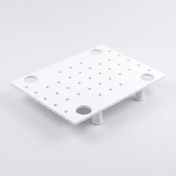
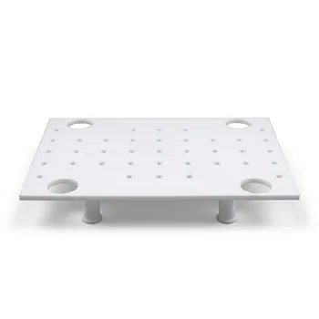
- High Temperature Resistant PTFE Thermal Insulation Board Corrosion Resistant Metal Free Fluoropolymer Stand for Ultra Clean Laboratories
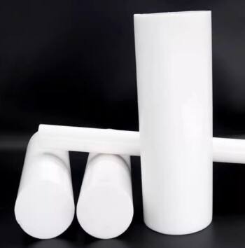
- Customizable PTFE Rods for Advanced Industrial Applications
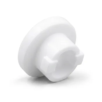
- Custom PTFE Insulating Gaskets Corrosion Resistant Teflon Seals Tailored Engineering Plastic Components
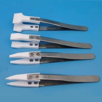
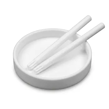
- Custom PTFE Parts Manufacturer for Teflon Parts and PTFE Tweezers
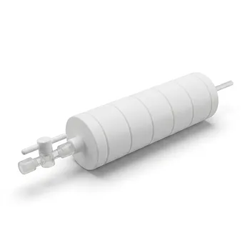
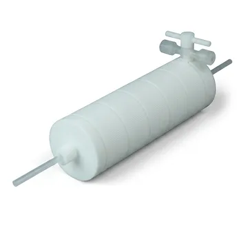
- PTFE Corrosion Resistant Filter with PFA Valve Connections and Integrated Sieve Plate
People Also Ask
- What are the common applications of PTFE bars? Key Uses in High-Performance Industries
- What are the limitations of pure PTFE in high temperature applications? Understanding the 200°C Ceiling
- Why are PTFE bars considered essential in modern industrial applications? Unlock Unmatched Chemical & Thermal Resistance
- What advantages do PTFE bars offer in chemical industries? Ensure Safety and Efficiency in Demanding Applications
- What are the primary applications of PTFE bars in the chemical industry? Solve Your Toughest Corrosion Problems