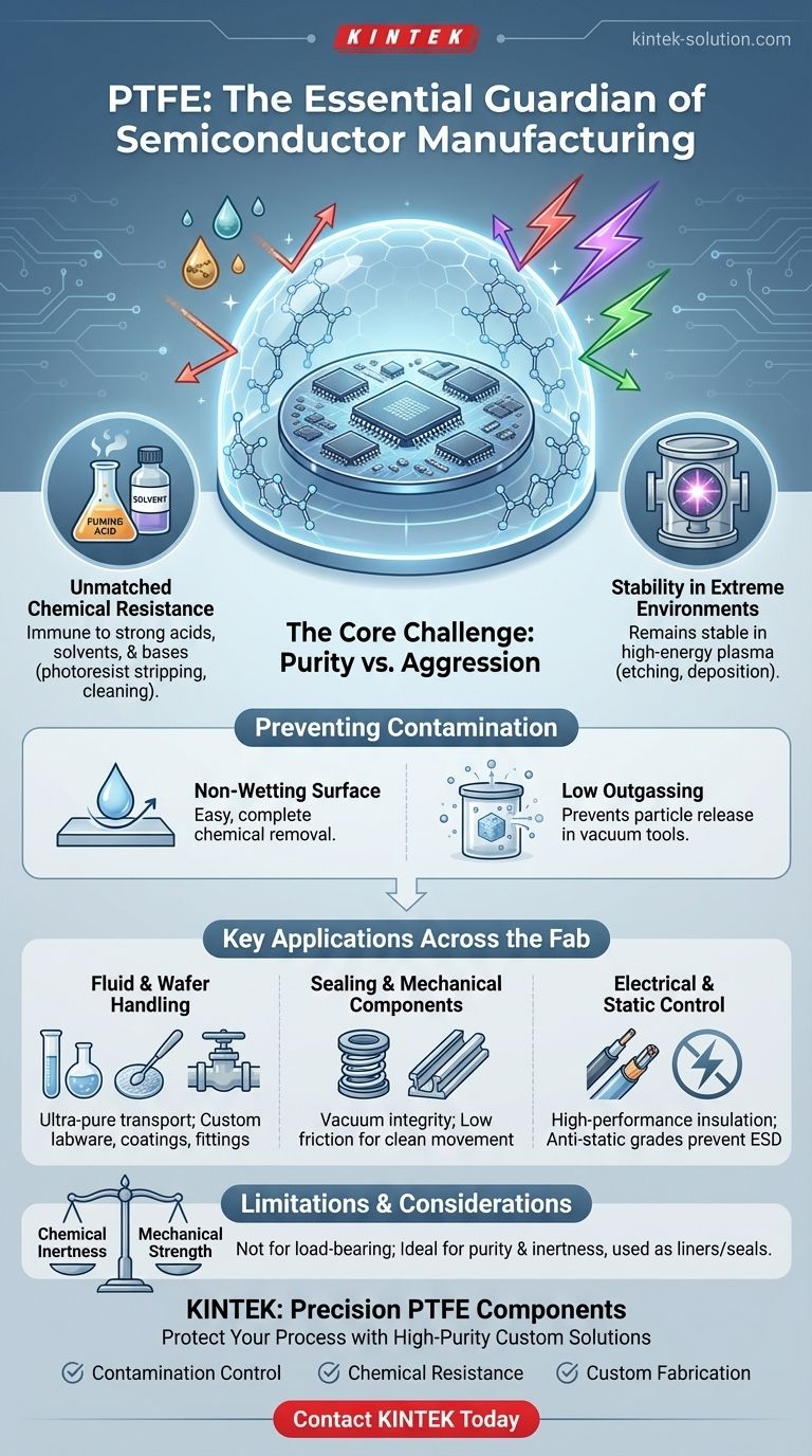
At its core, Polytetrafluoroethylene (PTFE) is a critical enabling material in semiconductor manufacturing. Its primary function is to serve as a barrier, preventing the highly corrosive chemicals essential for chip production from contaminating the ultra-clean manufacturing environment and damaging sensitive equipment. This ensures the purity and integrity of every step, from wafer handling to final processing.
The central challenge in semiconductor fabrication is achieving atomic-level perfection in an environment filled with aggressive chemicals. PTFE is indispensable because its unique combination of extreme chemical inertness, high purity, and stability allows it to withstand this environment without degrading or introducing contaminants.
The Core Challenge: Purity and Chemical Aggression
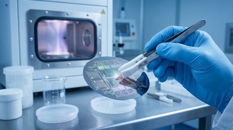
Semiconductor manufacturing operates on a scale where a single microscopic particle can render a multi-million dollar batch of microchips useless. The processes required to build these intricate circuits, such as photolithography and etching, rely on some of the most aggressive substances used in any industry.
Unmatched Chemical Resistance
PTFE is virtually immune to the strong acids, solvents, and bases used throughout the fabrication process.
This property is crucial for components that directly handle these chemicals, such as in the photoresist stripping and wafer cleaning stages, where its non-reactive nature prevents it from leaching impurities.
Stability in Extreme Environments
Modern chipmaking relies on plasma, an energized gas, for processes like etching and thin-film deposition.
PTFE remains chemically stable even when exposed to these high-energy plasma environments, making it one of the few materials suitable for components inside process chambers.
Preventing Particulate Contamination
Contamination is the primary enemy of yield in a semiconductor fab. PTFE helps combat this in two key ways.
First, its non-wetting surface means chemical residues can be removed easily and completely, preventing cross-contamination between process steps. Second, high-purity grades of PTFE exhibit extremely low outgassing, meaning they don't release particles or vapor when in a vacuum, a critical requirement for deposition and etching tools.
Key Applications Across the Fab
Because of these properties, PTFE is not used for just one purpose but is found in various forms throughout the manufacturing facility, or "fab."
Fluid and Wafer Handling
PTFE is fabricated into custom labware like wafer dippers and containers. It is also used as a coating or solid resin for pipes, valves, and fittings that transport ultra-pure water and corrosive chemicals, ensuring the fluid path remains pristine.
Sealing and Mechanical Components
In the vacuum chambers used for etching and deposition, PTFE spring-energized seals provide a reliable barrier. They maintain vacuum integrity while resisting aggressive process chemicals and minimizing contamination.
Its low-friction properties also make it ideal for guide rails and slide pads in wafer handling systems, allowing for smooth, clean mechanical movement.
Electrical and Static Control
PTFE is an excellent electrical insulator, used for high-performance cable insulation in cleanroom equipment.
Furthermore, specialized anti-static grades of PTFE are available. These are essential for components used in static-sensitive environments to prevent electrostatic discharge (ESD) from damaging the delicate circuits on the wafer.
Limitations and Considerations
While its chemical properties are unmatched, PTFE is not a universal solution. It is a relatively soft material with lower mechanical strength and creep resistance compared to metals or ceramics.
Therefore, its application is reserved for components where chemical inertness and purity are the primary requirements, not structural load-bearing capacity. Engineers must design around these mechanical limitations, often incorporating PTFE as a liner or seal within a more robust assembly.
Making the Right Choice for Your Application
Selecting the right material is a matter of matching its properties to the specific demands of the manufacturing step.
- If your primary focus is fluid handling purity: Use PTFE for linings, tubing, and containers where its chemical inertness and non-wetting surface will prevent contamination.
- If your primary focus is vacuum chamber integrity: Specify low-outgassing grades of PTFE for seals and internal components to maintain a clean, particle-free environment.
- If your primary focus is static control: Mandate anti-static PTFE for any component handling wafers or sensitive electronic assemblies to prevent ESD damage.
- If your primary focus is clean mechanical movement: Employ PTFE for slide pads and guide rails where low friction is needed without introducing lubricants or particulates.
Ultimately, PTFE acts as an invisible but essential guardian, protecting the incredibly complex and sensitive process of chip creation from chemical attack and contamination.
Summary Table:
| Key PTFE Property | Role in Semiconductor Manufacturing |
|---|---|
| Chemical Inertness | Resists aggressive acids, solvents, and bases used in cleaning and etching. |
| High Purity & Low Outgassing | Prevents contamination in ultra-clean and vacuum environments. |
| Plasma Stability | Maintains integrity in high-energy plasma etching and deposition chambers. |
| Non-Wetting Surface | Allows for complete chemical removal, preventing cross-contamination. |
| Low Friction | Enables clean mechanical movement in wafer handling systems without lubricants. |
Protect Your Semiconductor Manufacturing Process with Precision PTFE Components
PTFE is the guardian of purity in semiconductor fabs, but its performance depends on precise manufacturing. KINTEK specializes in high-purity PTFE components—including custom seals, liners, labware, and fluid handling parts—that meet the extreme demands of semiconductor, medical, and laboratory applications.
We ensure:
- Contamination Control: Our components are engineered for ultra-low outgassing and particulate generation.
- Chemical Resistance: Withstand the most aggressive process chemicals without degradation.
- Custom Fabrication: From prototypes to high-volume orders, we deliver solutions tailored to your specific requirements.
Ready to enhance your yield and protect your equipment? Contact KINTEB today to discuss your PTFE component needs.
Visual Guide
Related Products
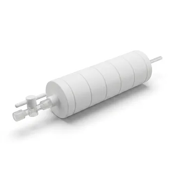
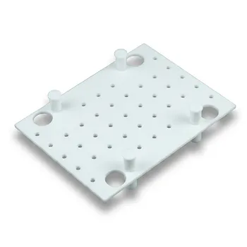
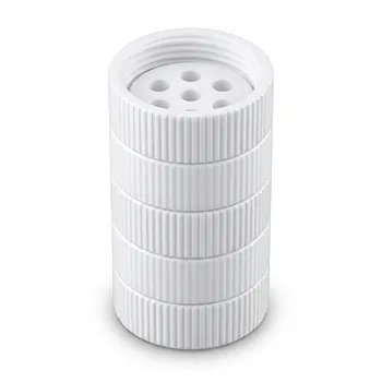
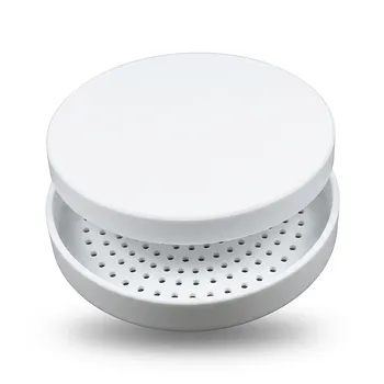
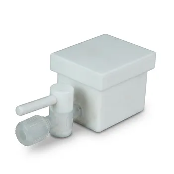
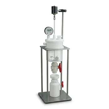
- Custom PTFE Filtration System Acid Resistant High Purity Semiconductor Grade Chemical Processing Filter
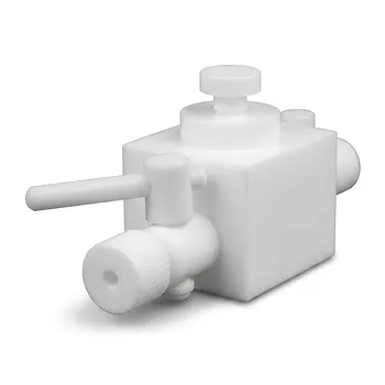
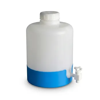
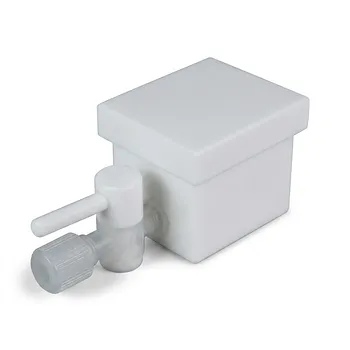
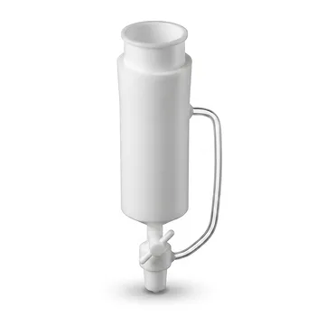
- High Corrosion Resistant PTFE Faucet Polytetrafluoroethylene Valve for Chemical Storage Drums and Fluid Transfer Systems Customizable Industrial Grade
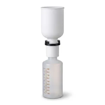
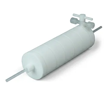
- PTFE PFA Vacuum Filtration System Corrosion Resistant Customizable Shatterproof Laboratory Device
- PTFE Corrosion Resistant Filter with PFA Valve Connections and Integrated Sieve Plate
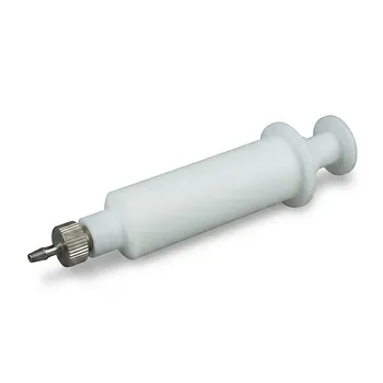
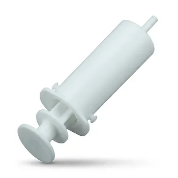
- High Temperature Chemical Resistant 50ml PTFE Syringe Customized Teflon Injector with Threaded Seal for Trace Analysis
People Also Ask
- What are the typical applications of PTFE filters in scientific filtration? Master Harsh Chemical and Gas Filtration
- Why are Polytetrafluoroethylene (PTFE) filters preferred for pharmaceutical and laboratory bioprocessing applications?
- Why are PTFE filters advantageous for gravimetric analysis? Achieve Unmatched Accuracy and Precision
- What makes PTFE filtration systems advantageous for industrial and scientific use? Unmatched Chemical & Thermal Stability
- What sizes and pore options are available for PTFE filters? Choose the Right Filter for Your Application