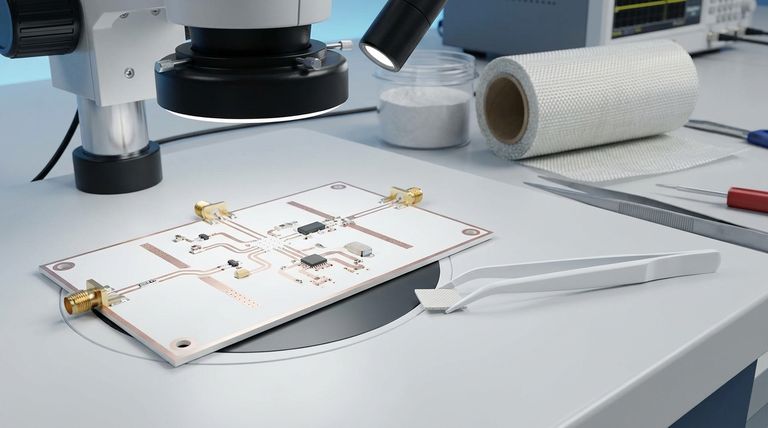
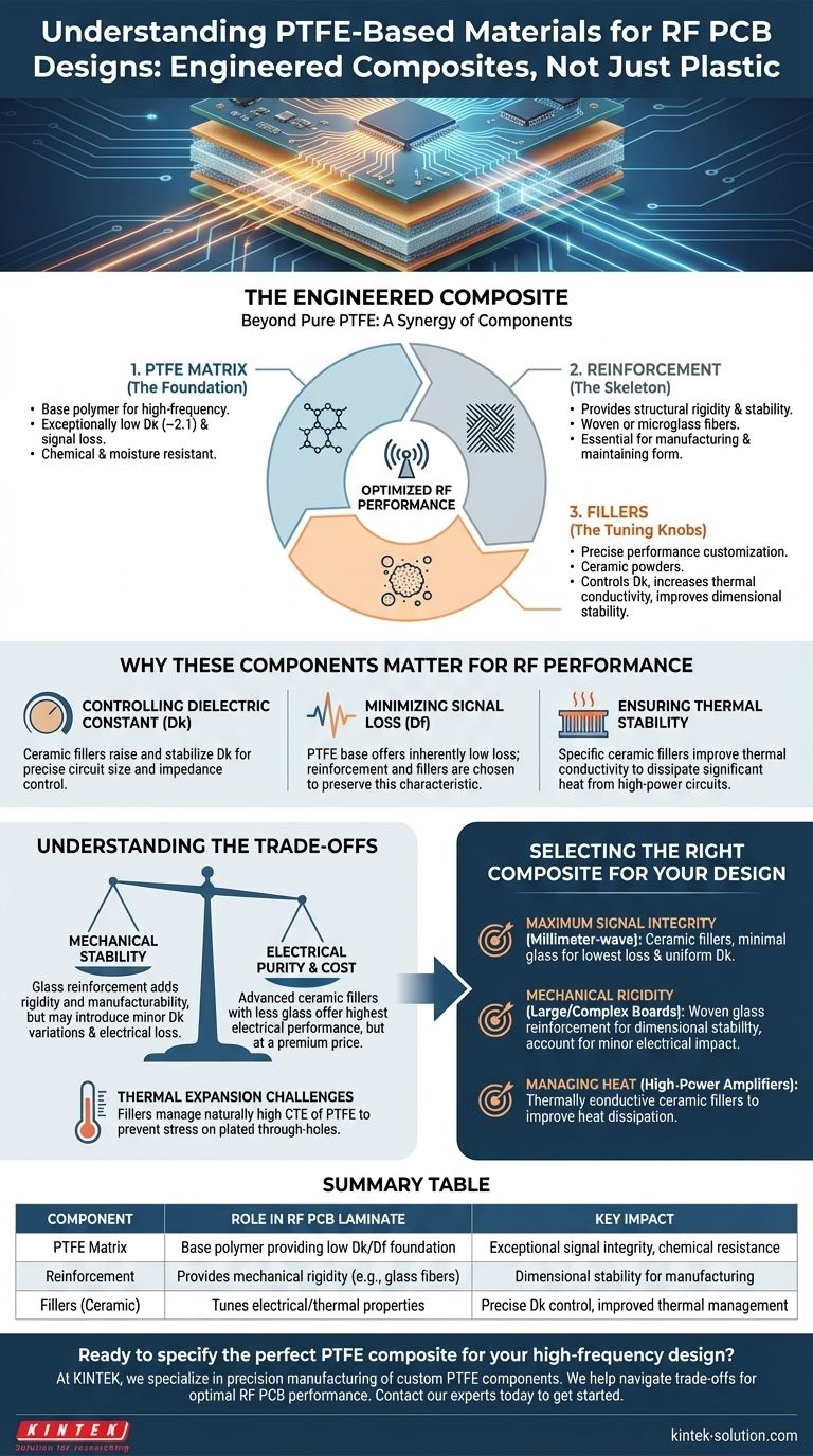
The primary components of PTFE-based materials for RF printed circuit boards (PCBs) are not just pure Polytetrafluoroethylene (PTFE). Instead, they are advanced composites consisting of a PTFE matrix, a structural reinforcement, and specialized fillers. The reinforcement provides mechanical rigidity, while fillers, typically ceramic powders, are used to precisely engineer the material's final electrical and thermal properties.
The key takeaway is that you are not simply choosing PTFE; you are selecting an engineered composite material. The true value lies in how the specific reinforcement and filler additives modify the base PTFE to achieve the exact performance characteristics required for a high-frequency application.
The Three Foundational Components
To understand these materials, it's essential to break them down into their three core elements. Each serves a distinct and critical function in the final laminate.
The PTFE Matrix (The Foundation)
Pure PTFE is the base polymer for these laminates. It is chosen for its inherently superior properties for high-frequency signals.
It offers an exceptionally low dielectric constant (Dk) of around 2.1 and very low signal loss. It also provides excellent chemical inertness and moisture resistance, making it highly reliable.
Reinforcement (The Skeleton)
Pure PTFE is mechanically soft and dimensionally unstable with temperature changes. Reinforcement provides the necessary structure and rigidity.
This component, often woven glass or microglass fibers, gives the laminate the mechanical stability required to endure PCB manufacturing processes and maintain its form during operation.
Fillers (The Tuning Knobs)
Fillers are microscopic particles, most often ceramics, blended into the PTFE matrix. They are the most critical component for customizing the material's performance.
These additives are used to precisely control the dielectric constant, increase thermal conductivity to manage heat, and improve the overall dimensional stability of the composite.
Why These Components Matter for RF Performance
The interaction between the PTFE, reinforcement, and fillers directly dictates how well a circuit will perform at high frequencies. An engineer's choice of material is a strategic decision based on these effects.
Controlling the Dielectric Constant (Dk)
While pure PTFE has a very low Dk, many RF designs require higher, specific Dk values to control circuit size and impedance. Ceramic fillers are the primary tool used to raise and stabilize the Dk to a precise, predictable value across a wide range of frequencies.
Minimizing Signal Loss (Df)
The primary reason for using a PTFE base is its inherently low dissipation factor (Df), or signal loss. The type and amount of reinforcement and filler are carefully chosen to preserve this low-loss characteristic, ensuring maximum signal power is transmitted through the circuit.
Ensuring Thermal Stability
High-power RF circuits generate significant heat. Certain ceramic fillers are specifically chosen for their ability to improve the thermal conductivity of the material. This allows heat to spread and dissipate more effectively, preventing damage to sensitive components.
Understanding the Trade-offs
Selecting a PTFE-based material involves balancing competing engineering priorities. There is no single "best" material, only the right one for a specific application.
Mechanical Stability vs. Electrical Purity
Adding a woven glass reinforcement dramatically improves the material's rigidity and manufacturability. However, the glass weave can introduce minor, localized variations in the Dk and slightly increase electrical loss compared to a purely ceramic-filled composite.
Cost vs. Performance
Materials with more advanced ceramic fillers and less or no glass reinforcement typically offer the most consistent and highest electrical performance. This performance comes at a premium price point compared to more common glass-reinforced laminates.
Thermal Expansion Challenges
PTFE has a naturally high coefficient of thermal expansion (CTE). While fillers help control this, it's a critical factor to manage. A mismatch in expansion between the laminate and the copper plating can stress plated through-holes, impacting long-term reliability.
Selecting the Right Composite for Your Design
Your final choice depends entirely on the primary goal of your RF circuit.
- If your primary focus is maximum signal integrity at millimeter-wave frequencies: Choose a composite with ceramic fillers and minimal to no glass reinforcement to achieve the lowest possible loss and most uniform Dk.
- If your primary focus is mechanical rigidity for a large or complex board: A composite with woven glass reinforcement provides essential dimensional stability, though you must account for its minor impact on electrical performance.
- If your primary focus is managing heat in a high-power amplifier: Select a material with specific thermally conductive ceramic fillers designed to improve heat dissipation away from active components.
Understanding these components transforms material selection from a simple choice into a strategic engineering decision.
Summary Table:
| Component | Role in RF PCB Laminate | Key Impact |
|---|---|---|
| PTFE Matrix | Base polymer providing low Dk/Df foundation | Exceptional signal integrity, chemical resistance |
| Reinforcement | Provides mechanical rigidity (e.g., glass fibers) | Dimensional stability for manufacturing |
| Fillers (Ceramic) | Tunes electrical/thermal properties | Precise Dk control, improved thermal management |
Ready to specify the perfect PTFE composite for your high-frequency design?
At KINTEK, we specialize in the precision manufacturing of custom PTFE components—from seals and liners to complex labware and specialized parts. Our expertise is crucial for industries like semiconductor, medical, and laboratory, where material performance is non-negotiable.
We can help you navigate the trade-offs between mechanical stability, electrical purity, and thermal management to achieve optimal performance for your RF PCBs. Let's discuss your project requirements, from prototype to high-volume production.
Contact our experts today to get started.
Visual Guide
Related Products
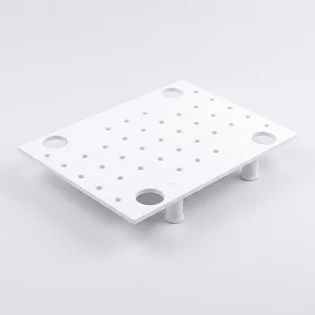
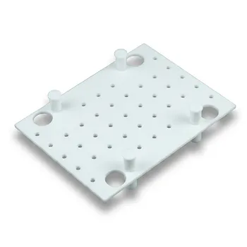
- High Temperature Resistant PTFE Thermal Insulation Board Corrosion Resistant Metal Free Fluoropolymer Stand for Ultra Clean Laboratories
- Customizable PTFE Heat Insulation Plate High Temperature Corrosion Resistant Laboratory Support Layered Multi Tier Stand
- Custom PTFE Multi Layer Filtration Plates Corrosion Resistant Low Background Lab Grade Filter Assemblies
- Custom PTFE Insulating Gaskets and Corrosion Resistant Fluoropolymer Seals for Industrial Electrical Applications
- PTFE Corrosion Resistant Filter with PFA Valve Connections and Integrated Sieve Plate
People Also Ask
- Can you provide examples of industries where PTFE bars have been successfully applied? Discover Key Applications
- What factors should be considered when choosing PTFE bars for chemical applications? Select the Right Grade for Your Process
- What are the common applications of PTFE bars? Key Uses in High-Performance Industries
- What materials are used to manufacture PTFE bars? A Guide to Virgin & Filled PTFE
- What are the limitations of pure PTFE in high temperature applications? Understanding the 200°C Ceiling