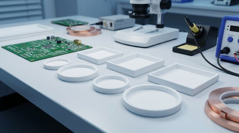
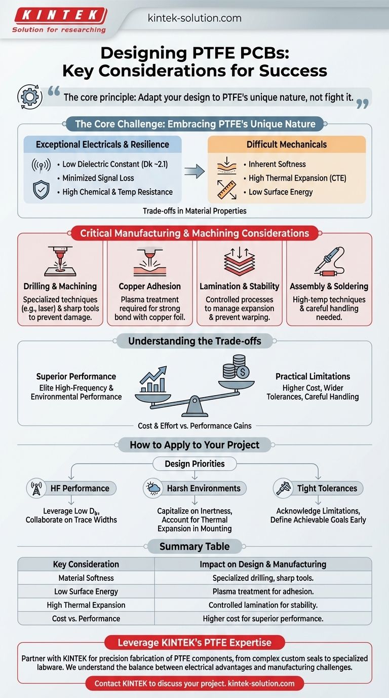
When designing a PTFE printed circuit board, you must account for its unique material properties at every stage, from layout to fabrication. The key considerations revolve around its inherent softness, high thermal expansion, and low surface energy, which necessitate specialized manufacturing processes for drilling, copper adhesion, and mechanical handling.
The core principle of successful PTFE PCB design is not to fight the material's nature but to adapt your design and manufacturing strategy to it. Success depends on accommodating its softness and thermal instability to leverage its exceptional high-frequency electrical performance.
The Core Challenge: Embracing PTFE's Unique Nature
Polytetrafluoroethylene (PTFE) is a high-performance material chosen for applications where standard substrates like FR-4 fail. Understanding its fundamental properties is the first step in a successful design.
Why Choose PTFE?
PTFE's primary advantage lies in its exceptional electrical properties. It has a very low and stable dielectric constant (Dk), around 2.1, which minimizes signal loss and ensures signal integrity in high-frequency applications like RF and microwave circuits.
It is also highly resistant to chemicals, moisture, and high temperatures, making it an ideal choice for PCBs deployed in harsh or demanding environments.
The Mechanical Paradox
The same molecular structure that gives PTFE its excellent electrical and chemical properties also makes it mechanically challenging. The material is very soft, prone to stress creep, and has a high coefficient of thermal expansion.
This means that while it's easy to machine in one sense, achieving and maintaining tight dimensional tolerances is significantly more difficult than with rigid materials.
Critical Manufacturing and Machining Considerations
A theoretical design is useless if it cannot be manufactured reliably. Your design choices must reflect the realities of PTFE fabrication.
Drilling and Machining
Because PTFE is so soft, standard drilling can easily damage the material, creating rough holes and poor plating surfaces. Specialized drilling techniques, such as high-resolution laser drilling, are often required.
When machining, use extremely sharp tools (HSS or carbide) at moderate speeds to prevent overheating and material deformation. Clamping pressure must be carefully controlled to avoid compressing or deforming the board.
Copper Adhesion and Plating
PTFE has very low surface energy, meaning other materials do not easily stick to it. This makes achieving strong adhesion between the copper layers and the PTFE substrate a major challenge.
Manufacturers use a plasma treatment process to etch the PTFE surface at a microscopic level, creating a rougher texture that allows for a strong mechanical bond with the copper foil.
Lamination and Dimensional Stability
The high thermal expansion of PTFE means the board will expand and contract significantly with temperature changes. This must be managed during the lamination of multi-layer boards to prevent warping and maintain layer-to-layer registration.
Controlled lamination processes and careful thermal management during fabrication are critical to ensuring the final board is dimensionally accurate.
Assembly and Soldering
The thermal stability of PTFE allows it to withstand high temperatures, but its softness can be a factor during assembly. Specialized high-temperature soldering techniques are often necessary to ensure reliable component connections without damaging the substrate.
Understanding the Trade-offs
Designing with PTFE is an exercise in balancing its superior performance with its practical limitations. Acknowledging these trade-offs is crucial for setting realistic project goals.
Cost vs. Performance
The specialized equipment, controlled processes, and experienced personnel required to fabricate PTFE PCBs make them significantly more expensive than standard FR-4 boards. This cost is a direct trade-off for its elite electrical and environmental performance.
Achieving Tight Tolerances
The combination of softness, stress creep, and a high coefficient of thermal expansion makes holding tight mechanical tolerances the single greatest challenge with PTFE. Designers must plan for more generous tolerances than they would with a rigid material.
Material Handling and Safety
PTFE is easily scratched or damaged. Careful handling throughout the entire fabrication and assembly process is essential. Furthermore, the micro-dust produced during machining can be hazardous if inhaled, requiring safety measures like masks or coolant systems.
How to Apply This to Your Project
Your design priorities will dictate which characteristics of PTFE demand the most attention.
- If your primary focus is high-frequency performance: Leverage the low Dk for clean signal integrity but collaborate closely with your fabricator to ensure trace width and spacing can be reliably produced.
- If your primary focus is reliability in harsh environments: Capitalize on PTFE's chemical inertness and thermal stability, but ensure your mechanical mounting design accounts for its high thermal expansion to prevent stress fractures.
- If your primary focus is achieving tight mechanical tolerances: Acknowledge that PTFE is not the ideal material for this and engage with your manufacturer early to define what is realistically achievable.
By understanding and designing with these characteristics, you can successfully harness the exceptional performance of PTFE for your most demanding applications.
Summary Table:
| Key Consideration | Impact on Design & Manufacturing |
|---|---|
| Material Softness | Requires specialized drilling (e.g., laser) and sharp tools to prevent damage. |
| Low Surface Energy | Demands plasma treatment for reliable copper adhesion. |
| High Thermal Expansion | Necessitates controlled lamination to prevent warping and maintain registration. |
| Cost vs. Performance | PTFE PCBs are more expensive but offer superior high-frequency and environmental performance. |
Ready to leverage PTFE's superior performance for your high-frequency, medical, or industrial application?
Designing and manufacturing a reliable PTFE PCB requires a partner with deep material expertise. KINTEK specializes in the precision fabrication of PTFE components, from complex custom seals and liners to specialized labware.
We understand the critical balance between PTFE's electrical advantages and its manufacturing challenges. Our team can help you navigate these complexities, offering support from prototype development to high-volume production.
Contact KINTERO today to discuss your project requirements and ensure your PTFE-based design is a success.
Visual Guide
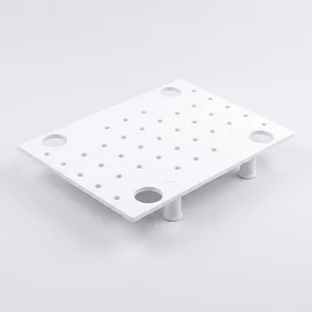
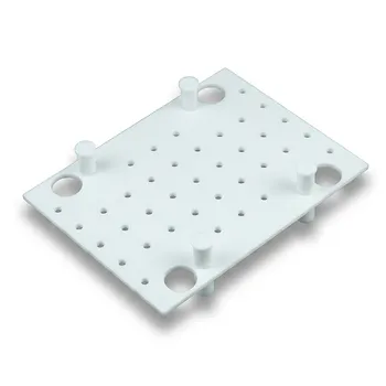
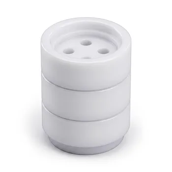
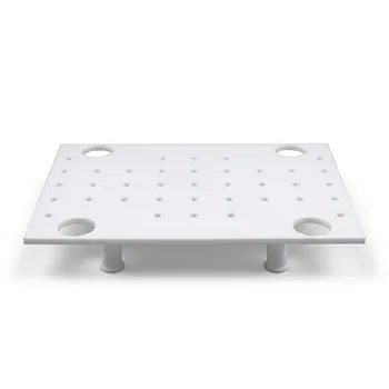
Related Products
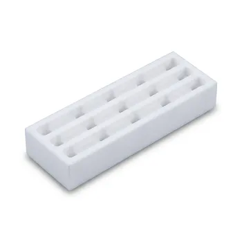
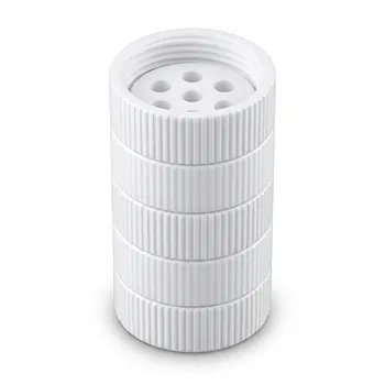
- High Temperature Resistant PTFE Thermal Insulation Board Corrosion Resistant Metal Free Fluoropolymer Stand for Ultra Clean Laboratories
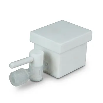
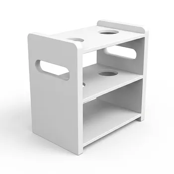
- Customizable PTFE Heat Insulation Plate High Temperature Corrosion Resistant Laboratory Support Layered Multi Tier Stand
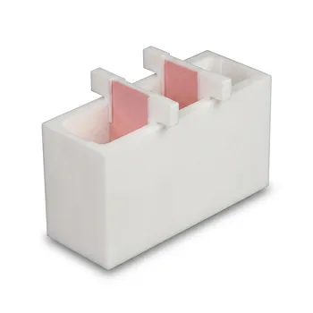
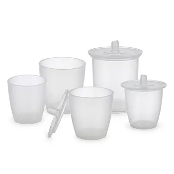
- Custom PTFE Multi Layer Filtration Plates Corrosion Resistant Low Background Lab Grade Filter Assemblies
- PTFE Anti Scald Heat Insulation Sleeve Hot Plate Support Feet Laboratory Benchtop Protection Customizable Thermal Barrier
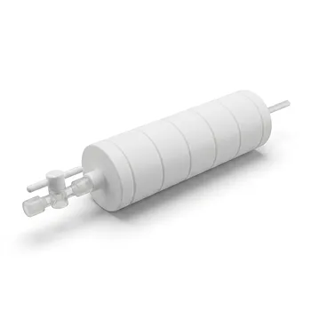
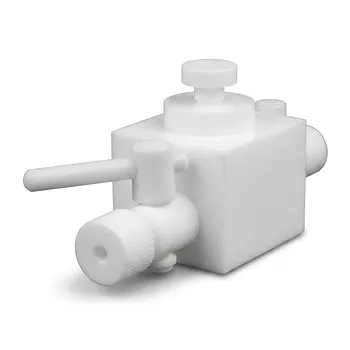
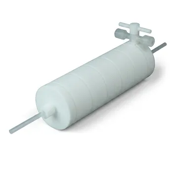
- PTFE Corrosion Resistant Filter with PFA Valve Connections and Integrated Sieve Plate
People Also Ask
- What are the primary applications of PTFE bars in the chemical industry? Solve Your Toughest Corrosion Problems
- What are some future trends in the application of PTFE bars in the chemical industry? Engineering for Extreme Performance
- What factors should be considered when choosing PTFE bars for chemical applications? Select the Right Grade for Your Process
- What are the common applications of PTFE bars? Key Uses in High-Performance Industries
- What are the limitations of pure PTFE in high temperature applications? Understanding the 200°C Ceiling