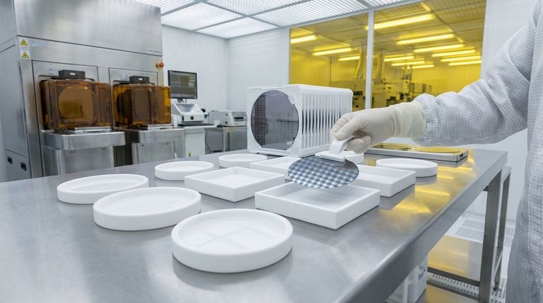
In the semiconductor industry, Polytetrafluoroethylene (PTFE) is a critical material used for components that must withstand extremely harsh chemical environments and wide temperature ranges without contaminating the manufacturing process. Due to its unique properties, it is specified in ultra-pure grades for applications like custom labware, fluid handling systems, and protective encapsulations for heating elements.
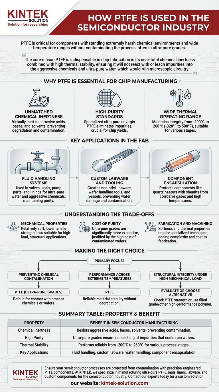
The core reason PTFE is indispensable in chip fabrication is its near-total chemical inertness combined with high thermal stability. These properties ensure that it will not react with or leach impurities into the aggressive chemicals and ultra-pure water used, which would otherwise ruin the microscopic circuitry on a silicon wafer.
Why PTFE is Essential for Chip Manufacturing
The environment inside a semiconductor fabrication plant, or "fab," is one of the most demanding on Earth. Materials must perform flawlessly under extreme conditions where even microscopic contamination can lead to catastrophic failure. PTFE's unique molecular structure makes it one of the few materials that can meet these demands.
Unmatched Chemical Inertness
Semiconductor manufacturing relies on a sequence of steps involving highly corrosive and reactive chemicals, including strong acids, bases, and solvents.
PTFE is virtually inert, meaning it does not react with these aggressive substances. This prevents the material from degrading and, more importantly, ensures it does not introduce contaminants into the process fluids.
High-Purity Standards
Standard-grade polymers are not suitable for semiconductor applications because they can contain fillers, processing aids, or other impurities that can leach out.
For this industry, specialized ultra-pure or virgin PTFE is used. This grade is manufactured to the highest purity standards to eliminate any risk of contamination that could affect chip yields.
Wide Thermal Operating Range
Chip fabrication involves processes that span a vast temperature spectrum, from cryogenic temperatures to several hundred degrees Celsius.
PTFE maintains its integrity and stability across an exceptionally broad range, typically from -200°C to 260°C (-328°F to 500°F), making it suitable for components used in various heating and cooling stages.
Key Applications in the Fab
PTFE's properties translate directly into specific, high-value applications throughout the semiconductor manufacturing process, particularly where purity and chemical resistance are paramount.
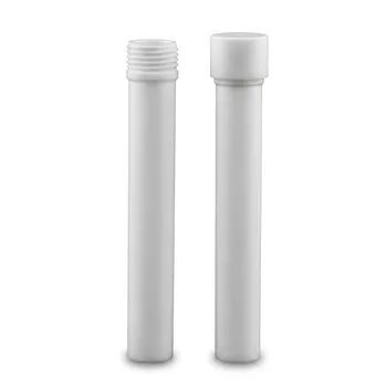
Fluid Handling Systems
The transport of ultra-pure water (UPW) and aggressive process chemicals is a critical function in a fab.
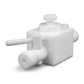
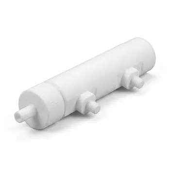
PTFE is used extensively for valves, seals, pump parts, and linings for hoses and pipes. Its non-reactive surface ensures the purity of the fluid it is transporting is maintained from the source to the point of use.
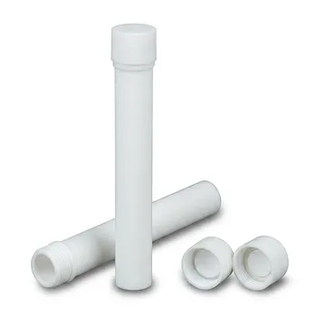
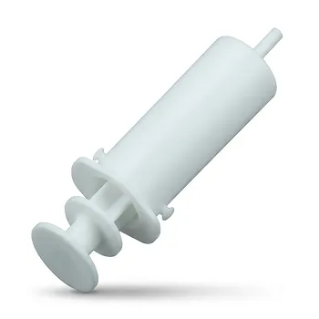
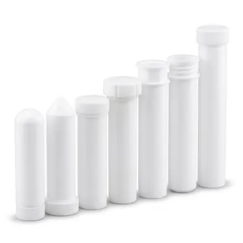
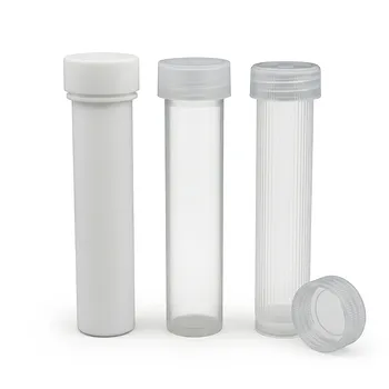
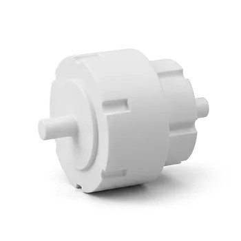
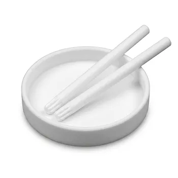
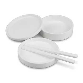
Custom Labware and Tooling
Any tool that comes into direct or indirect contact with a silicon wafer is a potential source of contamination.
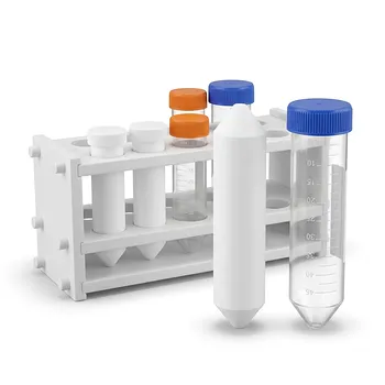
Because of its purity and non-stick properties, PTFE is used to create custom labware, wafer handling tools (like tweezers and grips), and process vessels. This ensures that wafers are not damaged or contaminated during handling and processing.
Component Encapsulation
Many components within process chambers must be protected from the harsh chemical environment.
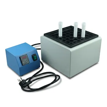
PTFE is used for encapsulation devices, such as protective sheaths for quartz heaters. The PTFE shield protects the heater from corrosive gases while withstanding the high operating temperatures.
Understanding the Trade-offs
While its properties make it ideal for many applications, PTFE is not a universal solution. Understanding its limitations is key to proper material selection.
Mechanical Properties
Compared to metals or other engineered polymers, PTFE is a relatively soft material with lower tensile strength and resistance to creep (deformation under constant load).
This makes it less suitable for high-load, structural applications where mechanical rigidity is the primary requirement.
Cost of Purity
The ultra-pure grades of PTFE required by the semiconductor industry are significantly more expensive than standard industrial grades.
This cost is justified by the immense expense of a single contaminated batch of wafers, making the investment in high-purity materials a necessary form of insurance.
Fabrication and Machining
While PTFE can be machined into complex shapes, its softness and thermal properties require specialized techniques to hold tight tolerances. This can add complexity and cost to the fabrication of custom parts.
Making the Right Choice for Your Process
Selecting the correct material is fundamental to ensuring process stability, maximizing yield, and avoiding costly downtime in semiconductor manufacturing.
- If your primary focus is preventing chemical contamination: PTFE's inertness and availability in ultra-pure grades make it the default choice for any surface in direct contact with process chemicals or wafers.
- If your primary focus is performance across extreme temperatures: For components exposed to the wide thermal cycles common in fabrication, PTFE provides reliable material stability without degradation.
- If your primary focus is structural integrity under high mechanical load: Carefully evaluate if PTFE's strength is sufficient, or if a filled grade of PTFE or a different high-performance polymer is necessary.
Ultimately, leveraging PTFE correctly is a foundational element of maintaining the pristine conditions required for modern chip fabrication.
Summary Table:
| Property | Benefit in Semiconductor Manufacturing |
|---|---|
| Chemical Inertness | Resists aggressive acids, bases, and solvents, preventing contamination. |
| High Purity | Ultra-pure grades ensure no leaching of impurities that could ruin wafers. |
| Thermal Stability | Performs reliably from -200°C to 260°C, suitable for various process stages. |
| Key Applications | Fluid handling systems, custom labware, wafer handling tools, and component encapsulation. |
Ensure your semiconductor processes are protected from contamination with precision-engineered PTFE components.
At KINTEK, we specialize in manufacturing ultra-pure PTFE seals, liners, labware, and custom components for the semiconductor, medical, and laboratory industries. Our expertise in precision production and custom fabrication—from prototypes to high-volume orders—ensures you receive components that meet the strictest purity and performance standards, safeguarding your yields and process integrity.
Contact our experts today to discuss your specific PTFE requirements and get a custom solution.
Visual Guide
Related Products
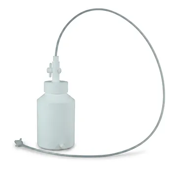
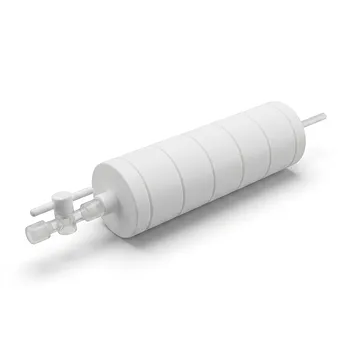
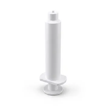
- Custom Virgin PTFE Gravity Leaching Pure Water System Corrosion Resistant Low Background Ultra High Purity Laboratory Processing Device
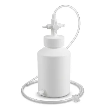
- High Purity PTFE Gravity Leaching System for Trace Analysis and Pure Water Filtration
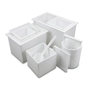
- High Purity PTFE Overflow Pickling Tank Integrated Seamless Polytetrafluoroethylene Laboratory Cleaning Sink
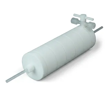
- High Purity PTFE Filter with PFA Valve Connections and Integrated Sieve Plate for Corrosive Fluid Processing
- High Purity PTFE Microwave Digestion Vessel Replacement for GT-400 Systems Acid Reflux and Sample Preparation
People Also Ask
- What processing methods are typically used for PTFE? Mastering the Unique Path from Powder to Precision Part
- How pure is virgin grade PTFE? The Definitive Guide to Non-Contaminating PTFE
- What is the significance of the low friction coefficient in PTFE processing machines? Enhance Quality and Machine Life
- How does PTFE's corrosion resistance benefit high-purity applications? Ensure Zero Contamination & System Integrity
- What are the challenges in processing PTFE? Overcoming High Melt Viscosity and Machining Difficulties