At its core, PTFE is adapted for semiconductor environments in two key ways: by leveraging its exceptional inherent properties, like chemical inertness and purity, and by formulating specialized grades, such as anti-static PTFE, to meet specific manufacturing demands. This dual approach allows the material to solve critical challenges related to chemical corrosion, electrostatic discharge (ESD), and process contamination that are unique to chip fabrication.
The suitability of PTFE for semiconductor manufacturing is not based on a single feature, but on a combination of its fundamental chemical stability and the availability of enhanced grades. Understanding which property solves which specific problem is the key to its effective application.
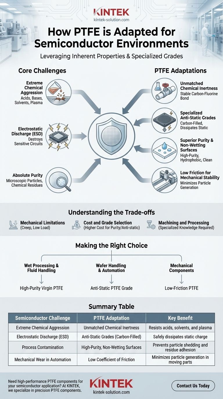
The Core Challenges of Semiconductor Environments
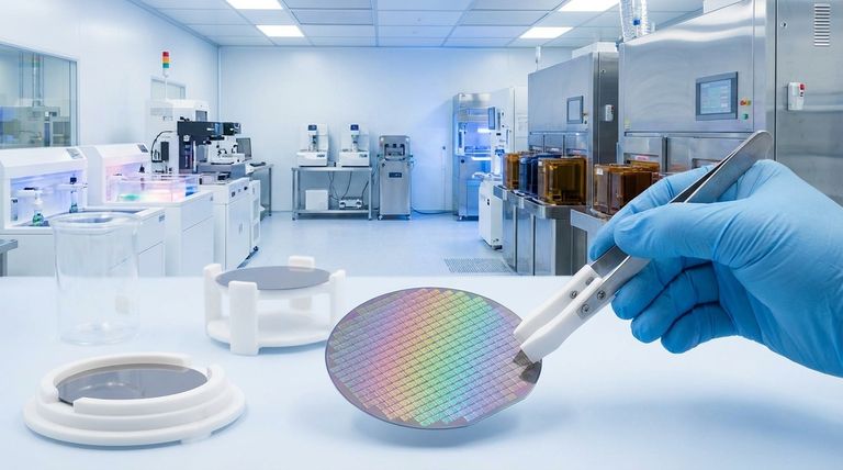
To understand why PTFE is so critical, we must first appreciate the uniquely hostile environment of a semiconductor fab. The processes involve a combination of extreme chemical aggression, sensitivity to static electricity, and an uncompromising need for purity.
Extreme Chemical Aggression
Semiconductor manufacturing relies on powerful chemicals for processes like etching and cleaning. These include highly corrosive acids, bases, and organic solvents that can degrade most materials on contact.
Component survival is non-negotiable. Any material used for fluid handling, wafer containers, or process chamber parts must be virtually immune to chemical attack.
The Threat of Electrostatic Discharge (ESD)
The microscopic circuits on a silicon wafer are incredibly sensitive to static electricity. A single, unseen electrostatic discharge event can permanently destroy a device, leading to significant yield loss.
Therefore, materials used in wafer handling and automation must not build up a static charge. They either need to be inherently conductive or specifically formulated to dissipate static safely.
The Mandate for Absolute Purity
Chip fabrication is a battle against contamination. Even microscopic particles or trace chemical residues can cause defects that render a chip useless.
Materials must not shed particles (outgassing) or absorb and later release chemical residues. Surfaces must be perfectly clean and, ideally, non-stick to prevent anything from adhering to them.
How PTFE Is Adapted to Solve These Challenges
PTFE, often known by the brand name Teflon®, is uniquely equipped to meet these demands. Its properties are not just beneficial; they are a direct solution to the industry's primary failure points.
Unmatched Chemical Inertness
The strength of the carbon-fluorine bond in PTFE makes it one of the most chemically non-reactive substances known. It is virtually immune to attack from the aggressive acids and solvents used in photoresist and etching processes.
This allows it to be used for tubing, valves, custom labware, and wafer dippers that are in direct contact with corrosive media, ensuring process integrity and equipment longevity. It even remains stable when exposed to plasma.
Superior Purity and Non-Wetting Surfaces
High-purity grades of PTFE are inherently clean and do not leach contaminants into the process environment. Furthermore, PTFE has excellent non-wetting and non-stick characteristics.
This "hydrophobic" nature is critical, as it allows for the complete removal of chemical residues during rinsing steps. This ensures no leftover reactants cross-contaminate the next stage, directly protecting product purity.
Low Friction for Mechanical Stability
In the automated machinery of a fab, moving parts like guide rails and slide pads must operate smoothly without generating particles. PTFE's extremely low coefficient of friction minimizes wear and prevents the creation of microscopic debris that could contaminate the cleanroom.
This property is also leveraged in cable insulation, where smooth, non-binding movement is required in robotic systems.
Specialized Anti-Static Grades
Standard PTFE is an excellent electrical insulator, which means it can accumulate a dangerous static charge. To solve this, anti-static grades of PTFE are produced.
These grades are formulated with a small amount of a conductive material, typically carbon, which allows static charge to dissipate safely and controllably. This adaptation makes PTFE a safe choice for ESD-sensitive applications like wafer containers and handling tools.
Understanding the Trade-offs
While highly effective, PTFE is not a universal solution. Acknowledging its limitations is key to proper material selection.
Mechanical Limitations
PTFE is a relatively soft material and can be prone to "creep," or deformation under sustained load. It is not suitable for high-load structural applications and is best used for its surface properties and chemical resistance in components like liners, seals, and low-load mechanical parts.
Cost and Grade Selection
High-purity and anti-static grades of PTFE are significantly more expensive than standard industrial grades. Using the wrong grade can be counterproductive—an industrial grade may introduce the very contaminants you are trying to avoid. Verification and certification of the material grade are essential.
Machining and Processing
Fabricating custom parts from PTFE requires specialized knowledge. The tools and techniques must be chosen to produce a smooth, clean surface finish without embedding contaminants into the soft material, which would negate its inherent purity.
Making the Right Choice for Your Application
Selecting the right type of PTFE requires matching its specific properties to your primary goal within the semiconductor process.
- If your primary focus is wet processing and fluid handling: Prioritize high-purity virgin PTFE for its unmatched chemical inertness and non-wetting surface to ensure process purity.
- If your primary focus is wafer handling and automation: Specify an anti-static PTFE grade to prevent electrostatic discharge while still benefiting from low friction and cleanliness.
- If your primary focus is mechanical components in cleanrooms: Use PTFE for its low-friction properties in guide rails or slide pads to minimize particle generation.
By understanding how to leverage PTFE's inherent strengths and specified adaptations, you can build more resilient, pure, and efficient semiconductor manufacturing processes.
Summary Table:
| Semiconductor Challenge | PTFE Adaptation | Key Benefit |
|---|---|---|
| Extreme Chemical Aggression | Unmatched Chemical Inertness | Resists acids, solvents, and plasma |
| Electrostatic Discharge (ESD) | Anti-Static Grades (Carbon-Filled) | Safely dissipates static charge |
| Process Contamination | High-Purity, Non-Wetting Surfaces | Prevents particle shedding and residue adhesion |
| Mechanical Wear in Automation | Low Coefficient of Friction | Minimizes particle generation in moving parts |
Need high-performance PTFE components for your semiconductor application?
At KINTEK, we specialize in manufacturing precision PTFE components—including seals, liners, labware, and custom parts—specifically for the semiconductor, medical, and laboratory industries. Our expertise ensures your components meet the stringent demands of chemical resistance, ESD safety, and ultra-purity.
We offer custom fabrication from prototypes to high-volume orders, guaranteeing that every part is tailored to solve your unique manufacturing challenges.
Contact us today to discuss your PTFE requirements and enhance your process reliability!
Visual Guide
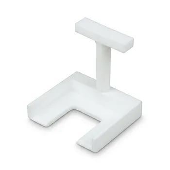
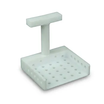
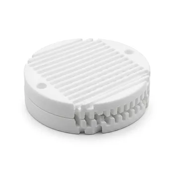
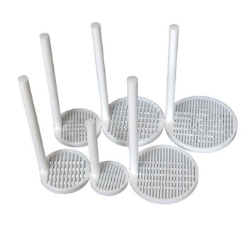
Related Products
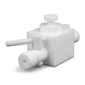
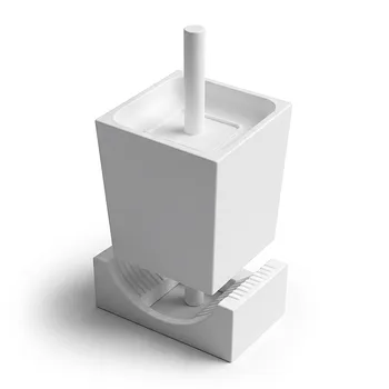
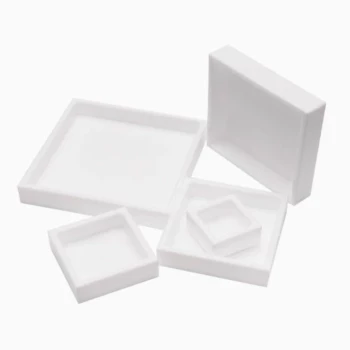
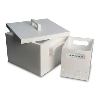
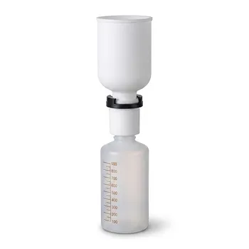
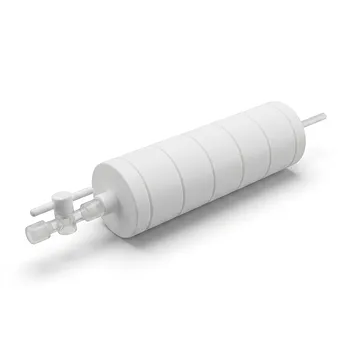
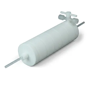
- Custom PTFE Filtration System Acid Resistant High Purity Semiconductor Grade Chemical Processing Filter
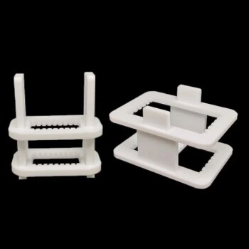
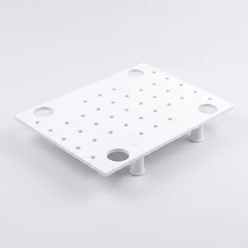
- Custom PTFE Wafer Cleaning Flower Basket Chemical Resistant Fluoropolymer Carrier for Semiconductor Etching and New Energy Processing
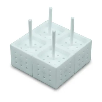
- High Purity PTFE Wafer Cassette Etching Carrier for Semiconductor Silicon Wafer Cleaning and Acid Resistance
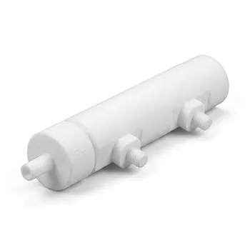
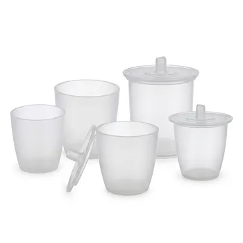
- High Purity Custom PTFE Reaction Cell Electrolytic Tank for Semiconductor and Polysilicon Industrial Applications
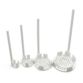
- PTFE Circular Wafer Carrier 6 Inch Acid Alkali Resistant Semiconductor Cleaning Basket Customizable
People Also Ask
- What temperature resistance do PTFE filters offer? Unmatched Thermal Stability from -200°C to +260°C
- How does the hydrophobicity of PTFE filters benefit their use? Ensure Uninterrupted Gas Flow and Solvent Filtration
- What are the typical applications of PTFE filters in scientific filtration? Master Harsh Chemical and Gas Filtration
- Why are Polytetrafluoroethylene (PTFE) filters preferred for pharmaceutical and laboratory bioprocessing applications?
- What sizes and pore options are available for PTFE filters? Choose the Right Filter for Your Application