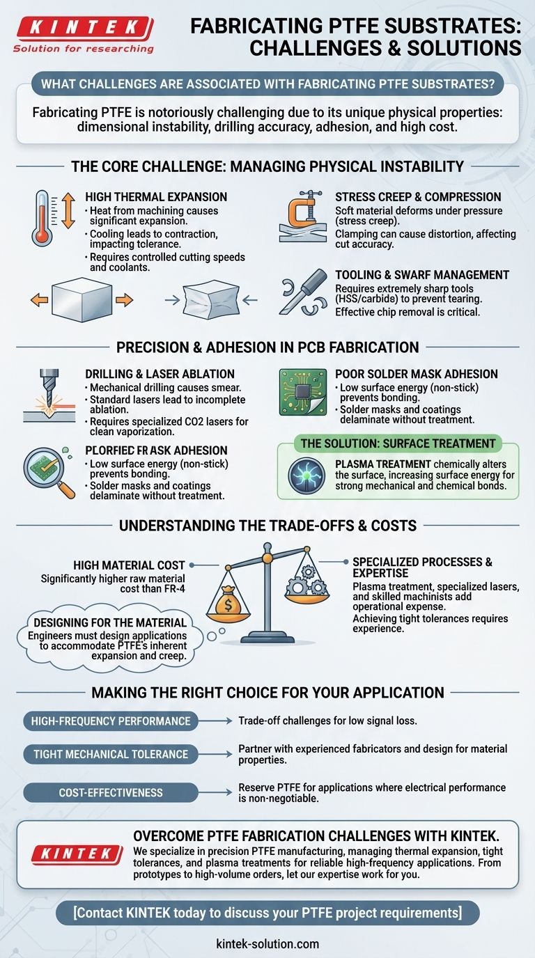
Fabricating PTFE substrates is notoriously challenging due to the material's unique combination of physical properties. The primary difficulties include managing its dimensional instability during machining, achieving accurate drilled holes, ensuring proper adhesion of surface layers like solder masks, and navigating its high material cost.
The core challenge with PTFE is not that it's difficult to cut, but that its inherent softness, high thermal expansion, and low surface energy make achieving precision and reliability exceptionally difficult without specialized tools, processes, and expertise.
The Core Challenge: Managing Physical Instability
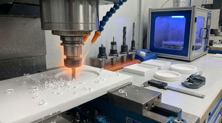
The primary fabrication issues stem from PTFE's physical nature. It is a soft material that reacts unpredictably to heat and pressure, which are unavoidable elements of machining and processing.
High Thermal Expansion
PTFE has a very high coefficient of thermal expansion. Heat generated from cutting tools causes the material to expand significantly during machining.
When the material cools, it contracts, often resulting in final dimensions that are out of the specified tolerance. This requires careful management of cutting speeds and the application of coolants.
Stress Creep and Compression
The material is soft and prone to deforming under pressure, a property known as stress creep.
When clamped for machining, it can easily be compressed. This makes it difficult to hold the substrate securely without distorting it, which directly impacts the accuracy of any cuts or drilled holes.
Tooling and Swarf Management
While PTFE's softness makes it seem easy to machine, it requires extremely sharp and polished cutting tools, preferably high-speed steel (HSS) or carbide.
Dull tools can tear or smear the material rather than cutting it cleanly. Effective swarf (chip) removal is also critical, as the soft cuttings can easily build up and compromise the surface finish.
Precision and Adhesion in PCB Fabrication
For electronics and printed circuit boards (PCBs), PTFE presents a unique set of challenges related to creating circuits and ensuring their durability.
Drilling and Laser Ablation
Achieving clean, precise holes is difficult. Mechanical drilling can cause material smear, while standard lasers can result in incomplete ablation.
This necessitates specialized processes, such as using CO2 lasers, which are better suited to vaporizing the material cleanly without excessive melting at the edges.
Poor Solder Mask Adhesion
PTFE is famous for its low surface energy, which is what makes it "non-stick." This same property is a major liability in PCB fabrication.
Solder masks, conformal coatings, and other essential layers will not bond properly to an untreated PTFE surface, leading to delamination and circuit failure.
The Solution: Surface Treatment
To overcome poor adhesion, the PTFE surface must be chemically altered.
This is typically done using a plasma treatment process, which etches the surface at a microscopic level. This increases its surface energy and creates a texture that allows for a strong mechanical and chemical bond with the solder mask.
Understanding the Trade-offs and Costs
Opting for PTFE is a decision that carries significant implications for both cost and complexity. It is not a drop-in replacement for standard materials like FR-4.
High Material Cost
The raw material cost of PTFE laminate is substantially higher than that of conventional PCB substrates. This establishes a high baseline cost before any fabrication begins.
Specialized Processes and Expertise
The need for plasma treatment, specialized lasers, and carefully controlled machining parameters adds significant operational expense.
Furthermore, success often depends on the skill of the machinist. Achieving tight tolerances (e.g., within +/- 0.002 inches) requires experience with PTFE's unique behavior, which is not universally available.
Designing for the Material
You cannot force a design intended for a rigid material onto PTFE. Engineers must design applications with PTFE's inherent properties in mind, accommodating its tendency to expand and creep.
Making the Right Choice for Your Application
Choosing to use PTFE requires a clear understanding of these challenges and their impact on your project's goals and budget.
- If your primary focus is high-frequency performance: The fabrication challenges are a necessary trade-off for PTFE's unmatched dielectric properties and low signal loss.
- If your primary focus is tight mechanical tolerance: You must partner with a fabricator experienced in PTFE and design components to accommodate the material's thermal expansion and stress creep.
- If your primary focus is cost-effectiveness: The combined material and processing costs mean PTFE should be reserved for applications where its electrical performance is absolutely non-negotiable.
Ultimately, successfully fabricating PTFE is about working with its properties, not against them.
Summary Table:
| Challenge | Key Issue | Impact on Fabrication |
|---|---|---|
| Physical Instability | High thermal expansion & stress creep | Dimensional inaccuracy, difficulty holding tolerances |
| Precision Machining | Soft material, requires sharp tools | Risk of tearing/smearing, needs specialized tooling |
| Adhesion | Low surface energy (non-stick) | Poor solder mask/coating adhesion, requires plasma treatment |
| Cost & Expertise | High material cost & specialized processes | Increased project expense, need for experienced fabricators |
Overcome PTFE Fabrication Challenges with KINTEK
Fabricating PTFE components doesn't have to be a struggle. At KINTEK, we specialize in precision PTFE manufacturing for the semiconductor, medical, laboratory, and industrial sectors. Our expertise in managing thermal expansion, achieving tight tolerances, and applying surface treatments like plasma etching ensures your high-frequency or specialized applications perform reliably.
We offer custom fabrication from prototypes to high-volume orders, working with you to design components that leverage PTFE's properties effectively.
Contact KINTEK today to discuss your PTFE project requirements and let our expertise work for you.
Visual Guide
Related Products
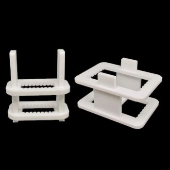
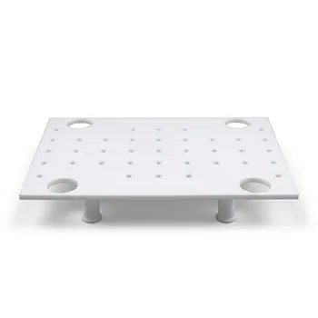
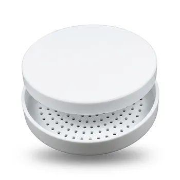
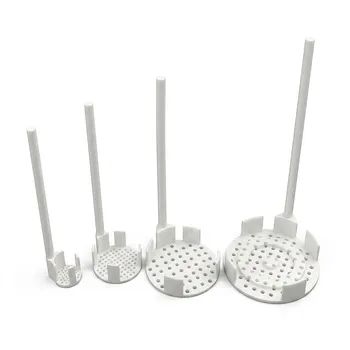
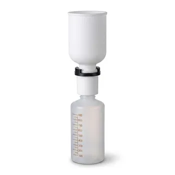
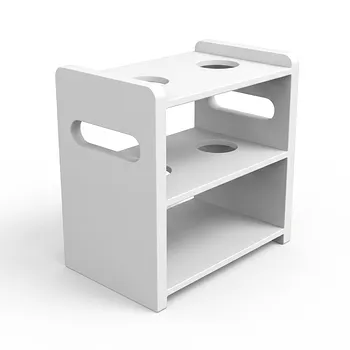
- Custom PTFE Teflon Parts Manufacturer Conductive Glass Substrate Cleaning Rack
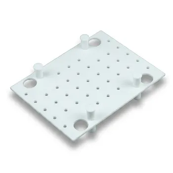
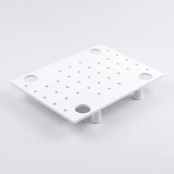
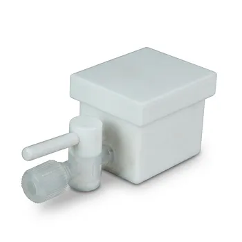
- Customizable PTFE Heat Insulation Plate High Temperature Corrosion Resistant Laboratory Support Layered Multi Tier Stand
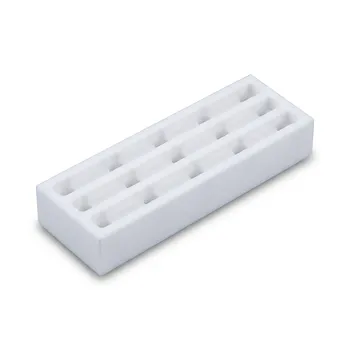
- Custom PTFE Multi Layer Filtration Plates Corrosion Resistant Low Background Lab Grade Filter Assemblies
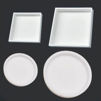
- High Temperature Resistant PTFE Thermal Insulation Board Corrosion Resistant Metal Free Fluoropolymer Stand for Ultra Clean Laboratories
- PTFE Anti Scald Heat Insulation Sleeve Hot Plate Support Feet Laboratory Benchtop Protection Customizable Thermal Barrier
People Also Ask
- What are the properties of glass-filled PTFE? Enhanced Strength & Wear Resistance for Demanding Applications
- What type of glass is used in glass-filled PTFE? The Definitive Answer for Superior Performance
- What structural components are typically found in a high-purity PTFE wafer cleaning rack? Optimize Your Cleaning Process
- How does glass-filled PTFE differ from pure PTFE? A Guide to Enhanced Mechanical Performance
- What are the advantages and disadvantages of glass-filled PTFE? A Guide to Enhanced Performance & Trade-offs